Описание
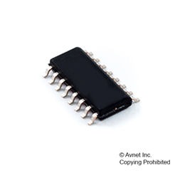
The ST7LITE0x is member of the ST7 microcontroller family. All ST7 devices are based on a common industry-standard 8-bit core, featuring an enhanced instruction set. The ST7LITE0x features FLASH memory with byte-by-byte In-Circuit Programming (ICP) and In-Application Programming (IAP) capability. Under software control, the ST7LITE0x device can be placed in WAIT, SLOW, or HALT mode, reducing power consumption when the application is in idle or standby state. The enhanced instruction set and addressing modes of the ST7 offer both power and flexibility to software developers, enabling the design of highly efficient and compact application code. In addition to standard 8-bit data management, all ST7 microcontrollers feature true bit manipulation, 8×8 unsigned multiplication and indirect addressing modes.
- Memories
- 1K or 1.5 Kbytes single voltage Flash Program memory with read-out protection, In-Circuit and In-Application Programming (ICP and IAP). 10 K write/erase cycles guaranteed, data retention: 20 years at 55 °C.
- 128 bytes RAM.
- 128 bytes data EEPROM with read-out protection. 300K write/erase cycles guaranteed, data retention: 20 years at 55 °C.
- Clock, Reset and Supply Management
- 3-level low voltage supervisor (LVD) and aux- iliary voltage detector (AVD) for safe power- on/off procedures
- Clock sources: internal 1MHz RC 1% oscillator or external clock
- PLL x4 or x8 for 4 or 8 MHz internal clock
- Four Power Saving Modes: Halt, Active-Halt, Wait and Slow
- Interrupt Management
- 10 interrupt vectors plus TRAP and RESET
- 4 external interrupt lines (on 4 vectors)
- I/O Ports
- 13 multifunctional bidirectional I/O lines
- 9 alternate function lines
- 6 high sink outputs
- 2 Timers
- One 8-bit Lite Timer (LT) with prescaler including: watchdog, 1 realtime base and 1 input capture.
- One 12-bit Auto-reload Timer (AT) with output compare function and PWM
- 1 Communication Interface
- SPI synchronous serial interface
- A/D Converter
- 8-bit resolution for 0 to VDD
- Fixed gain Op-amp for 11-bit resolution in 0 to 250 mV range (@ 5V VDD)
- 5 input channels
- Instruction Set
- 8-bit data manipulation
- 63 basic instructions with illegal opcode detection
- 17 main addressing modes
- 8 x 8 unsigned multiply instruction
- Development Tools
- Full hardware/software development package