Описание
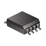
The LinkSwitch™-3 family of ICs dramatically simplifies low power CV/CC charger designs by eliminating an optocoupler and secondary control circuitry. The device introduces a revolutionary control technique to provide very accurate output voltage and current regulation, compen-sating for transformer and internal parameter tolerances along with input voltage variations.The device incorporates a 725 V power MOSFET, a novel ON/OFF control state machine, a high-voltage switched current source for self biasing, frequency jittering, cycle-by-cycle current limit and hysteretic thermal shutdown circuitry onto a monolithic IC.
- Dramatically Simplifies CV/CC Converters
- Eliminates optocoupler and all secondary CV/CC control circuitry
- Eliminates all control loop compensation circuitry
- Advanced Performance Features
- Compensates for transformer inductance tolerances
- Compensates for input line voltage variations
- Compensates for cable voltage drop
- Compensates for external component temperature variations
- Very accurate IC parameter tolerances using test trimming technology
- Frequency jittering greatly reduces EMI filter cost
- Programmable switching frequency up to 85 kHz to reduce transformer size
- Minimum operation frequency fixed to improve transient load response
- Advanced Protection/Safety Features
- Auto-restart protection reduces power delivered by >90% for output short-circuit and control loop faults (open and shorted components)
- Hysteretic thermal shutdown – automatic recovery reduces power supply returns from the field
- Meets high-voltage creepage requirements between DRAIN and all other pins both on the PCB and at the package


