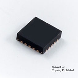
Multiplexer/Demultiplexer Bus Switch 1-Element CMOS 4-IN 20-Pin TQFN, TC7PCI3215MTLF, Toshiba

The TC7PCI3215MT is 2 differential channel, 1-2 multiplexer/demultiplexer for PCI Express Gen3 (8Gbps), or other high-speed interface applications. The An+/An- inputs is connected to the Bn+/Bn- or Cn+/Cn- outputs determined by the combination both the select input (SEL) and output enable (OE). When the output enable (OE) input is held high-level, the switches are open (high-impedance state) with regardless the state of select inputs and reducing consumption current. All inputs are equipped with protection circuits against static discharge.

  • Operating voltage: Vcc = 3.0 to 3.6 V
  • Switch terminal ON-capacitance: Ci/o = 1.5 pF Switch On (typ.) @Vcc = 3.3 V
  • ON resistance: Ron = 7.5 ? (typ.) @Vcc = 3.0 V, Vis = 0 V
  • -3dB Bandwidth: BW = 11.5 GHz (typ.) @ Vcc = 3.3 V
  • Insertion Loss: DDIL = -1 dB (typ.) @ Vcc = 3.3 V, f = 4 GHz
  • Off Isolation: DDOIRR = -20 dB (typ.) @ Vcc = 3.3 V, f = 4 GHz
  • Crosstalk: DDNEXT = -40 dB (typ.) @ Vcc = 3.3 V, f = 4 GHz
  • ESD performance: Machine model = ±200 V, Human body model = ±2000 V
  • Package: TQFN20

Характеристики

Бренд

Max_on_resistance

8.5 Ohm

Number_of_outputs_per_chip

4

Propagat_delay_test_condit

5 pF

Typical_operat_supply_volt

3.3 V

Max_quiescent_current

500 uA

Min_operating_supply_volt

3 V

Number_of_elements_per_chip

1

Logic_function

Multiplexer/Demultiplexer Bus Switch

Max_operating_supply_volt

3.6 V

Max_propagation_delay_time

0.1(Typ)@3.3V ns

Number_of_inputs_per_chip

4

Конфигурация

2 x 2:1

Eccn

EAR99

Htsn

8542390001

Mounting

Surface Mount

Operat_temperature

-40 to 85 °C

Pin_count

20

Product_dimensions

4.5 x 2.5 x 0.5(Max)

Schedule_b

8542390000

Screening_level

Industrial

Specifications

https://4donline.ihs.com/images/VipMasterIC/IC/TOSC/TOSC-S-A0001056701/TOSC-S-A0001059257-1.pdf?hkey=52A5661711E402568146F3353EA87419

Supplier_package

TQFN

Артикул: TC7PCI3215MTLF

Описание

The TC7PCI3215MT is 2 differential channel, 1-2 multiplexer/demultiplexer for PCI Express Gen3 (8Gbps), or other high-speed interface applications. The An+/An- inputs is connected to the Bn+/Bn- or Cn+/Cn- outputs determined by the combination both the select input (SEL) and output enable (OE). When the output enable (OE) input is held high-level, the switches are open (high-impedance state) with regardless the state of select inputs and reducing consumption current. All inputs are equipped with protection circuits against static discharge.

  • Operating voltage: Vcc = 3.0 to 3.6 V
  • Switch terminal ON-capacitance: Ci/o = 1.5 pF Switch On (typ.) @Vcc = 3.3 V
  • ON resistance: Ron = 7.5 ? (typ.) @Vcc = 3.0 V, Vis = 0 V
  • -3dB Bandwidth: BW = 11.5 GHz (typ.) @ Vcc = 3.3 V
  • Insertion Loss: DDIL = -1 dB (typ.) @ Vcc = 3.3 V, f = 4 GHz
  • Off Isolation: DDOIRR = -20 dB (typ.) @ Vcc = 3.3 V, f = 4 GHz
  • Crosstalk: DDNEXT = -40 dB (typ.) @ Vcc = 3.3 V, f = 4 GHz
  • ESD performance: Machine model = ±200 V, Human body model = ±2000 V
  • Package: TQFN20

Детали

Бренд

Max_on_resistance

8.5 Ohm

Number_of_outputs_per_chip

4

Propagat_delay_test_condit

5 pF

Typical_operat_supply_volt

3.3 V

Max_quiescent_current

500 uA

Min_operating_supply_volt

3 V

Number_of_elements_per_chip

1

Logic_function

Multiplexer/Demultiplexer Bus Switch

Max_operating_supply_volt

3.6 V

Max_propagation_delay_time

0.1(Typ)@3.3V ns

Number_of_inputs_per_chip

4

Конфигурация

2 x 2:1

Eccn

EAR99

Htsn

8542390001

Mounting

Surface Mount

Operat_temperature

-40 to 85 °C

Pin_count

20

Product_dimensions

4.5 x 2.5 x 0.5(Max)

Schedule_b

8542390000

Screening_level

Industrial

Specifications

https://4donline.ihs.com/images/VipMasterIC/IC/TOSC/TOSC-S-A0001056701/TOSC-S-A0001059257-1.pdf?hkey=52A5661711E402568146F3353EA87419

Supplier_package

TQFN