Описание
The SAL-XC866 is based on a high-performance 8-bit Central Processing Unit (CPU) that is compatible with the standard 8051 processor. While the standard 8051 processor is designed around a 12-clock machine cycle, the SAL-XC866 CPU uses a 2-clock machine cycle. This allows fast access to ROM or RAM memories without wait state. Access to the Flash memory, however, requires an additional wait state (one machine cycle). The instruction set consists of 45% one-byte, 41% two-byte and 14% three-byte instructions.
- High-performance XC800 Core
- On-chip memory
- I/O port supply at 3.3 V/5.0 V and core logic supply at 2.5 V (generated by embedded voltage regulator)
- Reset generation
- On-chip OSC and PLL for clock generation
- Power saving modes
- Programmable 16-bit Watchdog Timer (WDT)
- Four ports
- 8-channel, 10-bit ADC
- Three 16-bit timers
- Capture/compare unit for PWM signal generation (CCU6)
- Full-duplex serial interface (UART)
- Synchronous serial channel (SSC)
- On-chip debug support
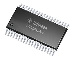
- PG-TSSOP-38 pin package