MCU 8-bit ST7 CISC 32KB Flash 2.5V/3.3V/5V 44-Pin LQFP, ST72F361J6T3, STMicroelectronics

The ST72361 devices are members of the ST7 microcontroller family designed for mid-range applications with LIN (Local Interconnect Network) interface. All devices are based on a common industrystandard 8-bit core, featuring an enhanced instruction set and are available with Flash or ROM program memory. The ST7 family architecture offers both power and flexibility to software developers, enabling the design of highly efficient and compact application code. The on-chip peripherals include an A/D converter, a PWM Autoreload timer, 2 general purpose timers, 2 asynchronous serial interfaces, and an SPI interface. For power economy, microcontroller can switch dynamically into WAIT, SLOW, Active-Halt, Auto Wake-up from HALT (AWU) or HALT mode when the application is in idle or stand-by state. Typical applications are consumer, home, office and industrial products.

  • Memories
    • 16K to 60K High Density Flash (HDFlash) or ROM with read-out protection capability. In
    • Application Programming and In-Circuit Programming for HDFlash devices
    • 1.5 to 2K RAM
    • HDFlash endurance: 100 cycles, data retention 40 years at 85°C
  • Clock, Reset and Supply Management
    • Low power crystal/ceramic resonator oscillators and bypass for external clock
    • PLL for 2x frequency multiplication
    • 5 power saving modes: Halt, Auto Wake Up From Halt, Active Halt, Wait and Slow
  • Interrupt Management
    • Nested interrupt controller
    • 14 interrupt vectors plus TRAP and RESET
    • TLI top level interrupt (on 64-pin devices)
    • Up to 21 external interrupt lines (on 4 vectors)
  • Up to 48 I/O Ports
    • Up to 48 multifunctional bidirectional I/O lines
    • Up to 36 alternate function lines
    • Up to 6 high sink outputs
  • 5 Timers
    • 16-bit timer with 2 input captures, 2 output compares, external clock input, PWM and pulse generator modes
    • 8-BIT timer with 1 or 2 input captures, 1 or 2 output compares, PWM and pulse generator modes
    • 8-BIT PWM auto-reload timer with 1 or 2 input captures, 2 or 4 independent PWM output channels, output compare and time base interrupt, external clock with event detector
    • Main clock controller with real-time base and clock output
    • Window watchdog timer
  • Up to 3 Communications Interfaces
    • SPI synchronous serial interface
    • Master/slave LINSCI™ asynchronous serial interface
    • Master
    • only LINSCI™ asynchronous serial interface
  • Analog Peripheral (Low Current Coupling)
    • 10-bit A/D converter with up to 16 inputs
    • Up to 9 robust ports (low current coupling)
  • Instruction Set
    • 8-BIT data manipulation
    • 63 basic instructions
    • 17 main addressing modes
    • 8 x 8 unsigned multiply instruction
  • Development Tools
    • Full hardware/software development package
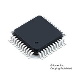
Характеристики

Бренд

Pin_count

44

Min_operating_supply_voltage

1.8 V

Max_operating_supply_voltage

5.5 V

Supplier_package

LQFP

Specifications

https://4donline.ihs.com/images/VipMasterIC/IC/SGST/SGST-S-A0002471722/SGST-S-A0002471722-1.pdf?hkey=52A5661711E402568146F3353EA87419

Schedule_b

8542310000

Ram_size

1.5 KB

Program_memory_type

Flash

Program_memory_size

32 Kb

Product_dimensions

10 x 10 x 1.4 mm

Operating_temperature

-40 to 85 °C

Data_bus_width

8 Bit

Operating_supply_voltage

2.5, 3.3, 5 V

On_chip_adc

11-chx10-bit

Number_of_timers

2

Number_of_programmable_i_os

39

Mounting

Surface Mount

Maximum_speed

12 MHz

Lead_finish

Tin/Lead

Instruction_set_architecture

CISC

Htsn

8542310001

Eccn

EAR99

Max_expanded_memory_size

64 KB

Артикул: ST72F361J6T3

Описание

The ST72361 devices are members of the ST7 microcontroller family designed for mid-range applications with LIN (Local Interconnect Network) interface. All devices are based on a common industrystandard 8-bit core, featuring an enhanced instruction set and are available with Flash or ROM program memory. The ST7 family architecture offers both power and flexibility to software developers, enabling the design of highly efficient and compact application code. The on-chip peripherals include an A/D converter, a PWM Autoreload timer, 2 general purpose timers, 2 asynchronous serial interfaces, and an SPI interface. For power economy, microcontroller can switch dynamically into WAIT, SLOW, Active-Halt, Auto Wake-up from HALT (AWU) or HALT mode when the application is in idle or stand-by state. Typical applications are consumer, home, office and industrial products.

  • Memories
    • 16K to 60K High Density Flash (HDFlash) or ROM with read-out protection capability. In
    • Application Programming and In-Circuit Programming for HDFlash devices
    • 1.5 to 2K RAM
    • HDFlash endurance: 100 cycles, data retention 40 years at 85°C
  • Clock, Reset and Supply Management
    • Low power crystal/ceramic resonator oscillators and bypass for external clock
    • PLL for 2x frequency multiplication
    • 5 power saving modes: Halt, Auto Wake Up From Halt, Active Halt, Wait and Slow
  • Interrupt Management
    • Nested interrupt controller
    • 14 interrupt vectors plus TRAP and RESET
    • TLI top level interrupt (on 64-pin devices)
    • Up to 21 external interrupt lines (on 4 vectors)
  • Up to 48 I/O Ports
    • Up to 48 multifunctional bidirectional I/O lines
    • Up to 36 alternate function lines
    • Up to 6 high sink outputs
  • 5 Timers
    • 16-bit timer with 2 input captures, 2 output compares, external clock input, PWM and pulse generator modes
    • 8-BIT timer with 1 or 2 input captures, 1 or 2 output compares, PWM and pulse generator modes
    • 8-BIT PWM auto-reload timer with 1 or 2 input captures, 2 or 4 independent PWM output channels, output compare and time base interrupt, external clock with event detector
    • Main clock controller with real-time base and clock output
    • Window watchdog timer
  • Up to 3 Communications Interfaces
    • SPI synchronous serial interface
    • Master/slave LINSCI™ asynchronous serial interface
    • Master
    • only LINSCI™ asynchronous serial interface
  • Analog Peripheral (Low Current Coupling)
    • 10-bit A/D converter with up to 16 inputs
    • Up to 9 robust ports (low current coupling)
  • Instruction Set
    • 8-BIT data manipulation
    • 63 basic instructions
    • 17 main addressing modes
    • 8 x 8 unsigned multiply instruction
  • Development Tools
    • Full hardware/software development package
Детали

Бренд

Pin_count

44

Min_operating_supply_voltage

1.8 V

Max_operating_supply_voltage

5.5 V

Supplier_package

LQFP

Specifications

https://4donline.ihs.com/images/VipMasterIC/IC/SGST/SGST-S-A0002471722/SGST-S-A0002471722-1.pdf?hkey=52A5661711E402568146F3353EA87419

Schedule_b

8542310000

Ram_size

1.5 KB

Program_memory_type

Flash

Program_memory_size

32 Kb

Product_dimensions

10 x 10 x 1.4 mm

Operating_temperature

-40 to 85 °C

Data_bus_width

8 Bit

Operating_supply_voltage

2.5, 3.3, 5 V

On_chip_adc

11-chx10-bit

Number_of_timers

2

Number_of_programmable_i_os

39

Mounting

Surface Mount

Maximum_speed

12 MHz

Lead_finish

Tin/Lead

Instruction_set_architecture

CISC

Htsn

8542310001

Eccn

EAR99

Max_expanded_memory_size

64 KB