Описание
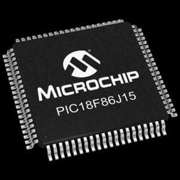
PIC18F86J15 is a new line of low-voltage devices with the main traditional advantage of all PIC18 microcontrollers – namely, high computational performance and a rich feature set – at an extremely competitive price point. These features make the PIC18F87J10 family a logical choice for many high-performance applications where cost is a primary consideration. All of the devices in the PIC18F87J10 family incorporate a range of features that can significantly reduce power consumption during operation. Alternate Run Modes: By clocking the controller from the Timer1 source or the internal RC oscillator, power consumption during code execution can be reduced by as much as 90%. Multiple Idle Modes: The controller can also run with its CPU core disabled but the peripherals still active. In these states, power consumption can be reduced even further, to as little as 4% of normal operation requirements On-the-Fly Mode Switching: The power-managed modes are invoked by user code during operation, allowing the user to incorporate power-saving ideas into their application’s software design. All of the devices in the PIC18F87J10 family offer five different oscillator options, allowing users a range of choices in developing application hardware. Two Crystal modes, using crystals or ceramic resonators. Two External Clock modes, offering the option of a divide-by-4 clock output. A Phase Lock Loop (PLL) frequency multiplier, available to the external oscillator modes which allows clock speeds of up to 40 MHz. An internal RC oscillator with a fixed 31-kHz output which provides an extremely low-power option for timing-insensitive applications The internal oscillator block provides a stable reference source that gives the family additional features for robust operation: Fail-Safe Clock Monitor: This option constantly monitors the main clock source against a reference signal provided by the internal oscillator. If a clock failure occurs, the controller is switched to the internal oscillator, allowing for continued low-speed operation or a safe application shutdown. Two-Speed Start-up: This option allows the internal oscillator to serve as the clock source from Power-on Reset, or wake-up from Sleep mode, until the primary clock source is available. The PIC18F87J10 family provides ample room for application code, from 32 Kbytes to 128 Kbytes of code space. The Flash cells for program memory are rated to last up to 100 erase/write cycles. The PIC18F87J10 family also provides plenty of room for dynamic application data, with up to 3936 bytes of data RAM In the unlikely event that 128 Kbytes of memory are inadequate for an application, the 80-pin members of the PIC18F87J10 family also implement an external memory bus. This allows the controller’s internal program counter to address a memory space of up to 2 Mbytes, permitting a level of data access that few 8-bit devices can claim. This allows additional memory options, including: Using combinations of on-chip and external memory up to the 2-Mbyte limit Using external Flash memory for reprogrammable application code or large data tables Using external RAM devices for storing large amounts of variable data The PIC18F87J10 family implements the optional extension to the PIC18 instruction set, adding 8 new instructions and an Indexed Addressing mode. Enabled as a device configuration option, the extension has been specifically designed to optimize re-entrant application code originally developed in high-level languages, such as ‘C’
- Operating Voltage Range: 2.0V to 3.6V
- 5.5V Tolerant Input (digital pins only)
- On Chip 2.5V Regulator
- Low Power, High Speed CMOS Flash Technology
- C Compiler Optimized Architecture:
- Optional extended instruction set designed to optimize re- entrant code
- Priority Levels for Interrupts
- 8 x 8 Single- Cycle Hardware Multiplier
- Extended Watchdog Timer (WDT):
- Programmable period from 4 ms to 131s
- Single- Supply In- Circuit Serial Programming™ (ICSP™) via Two Pins
- InCircuit Debug (ICD) with Three Break points via Two Pins
- Power- Managed modes:
- Run: CPU on, peripherals on
- Idle: CPU off, peripherals on
- Sleep: CPU off, peripherals off
- Flash Program Memory:
- 1000 erase/write cycle endurance typical
- 20 year retention minimum
- Self- write capability during normal operation Two Crystal modes, up to 40 MHz
- 4x Phase Lock Loop (PLL)
- Two External Clock modes, up to 40 MHz
- Internal 31 kHz Oscillator
- Secondary Oscillator using Timer1 @ 32 kHz
- Two- Speed Oscillator Start- up
- Fail- Safe Clock Monitor:
- Allows for safe shutdown if peripheral clock stops High- Current Sink/Source 25 mA/25 mA (PORTB and PORTC)
- Four Programmable External Interrupts
- Four Input Change Interrupts
- Two Capture/Compare/PWM (CCP) modules
- Three Enhanced Capture/Compare/PWM (ECCP) modules:
- One, two or four PWM outputs
- Selectable polarity
- Programmable dead time
- Auto- shutdown and auto- restart
- Two Master Synchronous Serial Port (MSSP) modules Supporting 3 Wire SPI (all 4 modes) and I2C™ Master and Slave modes
- Two Enhanced Addressable USART modules:
- Supports RS 485, RS 232 and LIN/2602
- Auto wake up on Start bit
- Auto Baud Detect (ABD)
- 10 Bit, up to 15 Channel Analog to Digital Converter module (A/D):
- Auto acquisition capability
- Conversion available during Sleep
- Self calibration feature
- Dual Analog Comparators with Input Multiplexing
- Address Capability of up to 2 Mbytes
- 8- Bit or 16- Bit Interface
- 12- Bit, 16- Bit and 20- Bit Addressing modes