Описание
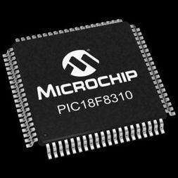
PIC18F8310 offers the advantages of all PIC18 microcontrollers – namely, high computational performance at an economical price. In addition to these features, the PIC18F6310/6410/8310/8410 family introduces design enhancements that make these microcontrollers a logical choice for many high-performance, power-sensitive applications. All of the devices in the PIC18F6310/6410/8310/8410 family incorporate a range of features that can significantly reduce power consumption during operation. Alternate Run Modes: By clocking the controller from the Timer1 source or the internal oscillator block, power consumption during code execution can be reduced by as much as 90%. Multiple Idle Modes: The controller can also run with its CPU core disabled, but the peripherals still active. In these states, power consumption can be reduced even further – to as little as 4% of normal operation requirements. On-the-Fly Mode Switching: The power-managed modes are invoked by user code during operation, allowing the user to incorporate power-saving ideas into their application’s software design Lower Consumption in Key Modules: The power requirements for both Timer1 and the Watchdog Timer have been reduced by up to 80%, with typical values of 1.1 µA and 2.1 µA, respectively. All of the devices in the PIC18F6310/6410/8310/8410 family offer nine different oscillator options, allowing users a wide range of choices in developing application hardware. Four Crystal modes, using crystals or ceramic resonators. Two External Clock modes, offering the option of using two pins (oscillator input and a divide-by-4 clock output) or one pin (oscillator input, with the second pin reassigned as general I/O). Two External RC Oscillator modes, with the same pin options as the External Clock modes. An internal oscillator block which provides an 8 MHz clock (±2% accuracy) and an INTRC source (approximately 31 kHz, stable over temperature and VDD), as well as a range of six user-selectable clock frequencies between 125 kHz to 4 MHz for a total of eight clock frequencies. This option frees the two oscillator pins for use as additional general purpose I/O. A Phase Lock Loop (PLL) frequency multiplier, available to both the High-Speed Crystal and Internal Oscillator modes, which allows clock speeds of up to 40 MHz. Used with the internal oscillator, the PLL gives users a complete selection of clock speeds from 31 kHz to 32 MHz – all without using an external crystal or clock circuit. Besides its availability as a clock source, the internal oscillator block provides a stable reference source that gives the family additional features for robust operation: Fail-Safe Clock Monitor: This option constantly monitors the main clock source against a reference signal provided by the internal oscillator. If a clock failure occurs, the controller is switched to the internal oscillator block, allowing for continued low-speed operation or a safe application shutdown. Two-Speed Start-up: This option allows the internal oscillator to serve as the clock source from Power-on Reset or wake-up from Sleep mode until the primary clock source is available
- Power-Managed Modes:
- Run: CPU on, Peripherals on
- Idle: CPU off, Peripherals on
- Sleep: CPU off, Peripherals off
- Ultra Low 50 nA Input Leakage
- Idle mode Currents Down to 2.3 µA Typical
- Ultra Low 50 nA Input Leakage
- Sleep mode Currents Down to 0.1 µA Typical
- Timer1 Oscillator: 1.0 µA, 32 kHz, 2V Typical
- Watchdog Timer: 1.7 µA Typical
- Two-Speed Oscillator Start-up Flexible Oscillator Structure:
- Four Crystal modes up to 40 MHz
- 4x Phase Lock Loop (available for crystal and internal oscillators)
- Two External RC modes, up to 4 MHz
- Two External Clock modes, up to 40 MHz
- Internal Oscillator Block:
- Fast wake from Sleep and Idle, 1 µs typical
- 8 user-selectable frequencies, from 31 kHz to 8 MHz
- Provides a complete range of clock speeds, from 31 kHz to 32 MHz, when used with PLL
- User-tunable to compensate for frequency drift
- Secondary Oscillator using Timer1 @ 32 kHz
- Fail-Safe Clock Monitor:
- Allows for safe shutdown if peripheral clock stops External Memory Interface (PIC18F8310/8410 Devices only):
- Address Capability of up to 2 Mbytes
- 16-Bit/8-Bit Interface
- Peripheral Highlights:
- High-Current Sink/Source 25 mA/25 mA
- Four External Interrupts
- Four Input Change Interrupts
- Four 8-Bit/16-Bit Timer/Counter modules
- Up to 3 Capture/Compare/PWM (CCP) modules
- Master Synchronous Serial Port (MSSP) module Supporting 3-Wire SPI (all 4 modes) and I2C™ Master and Slave modes
- Addressable USART module:
- Supports RS-485 and RS-232
- Enhanced Addressable USART module:
- Supports RS-485, RS-232 and LIN/J2602
- Auto-Wake-up on Start bit
- Auto-Baud Detect
- 10-Bit, up to 12-Channel Analog-to-Digital (A/D) Converter module:
- Auto-acquisition capability
- Conversion available during Sleep
- Dual Analog Comparators with Input Multiplexing
- Programmable 16-Level High/Low-Voltage Detection (HLVD) module:
- Supports interrupt on High/Low-Voltage Detection Special Microcontroller Features:
- C Compiler Optimized Architecture:
- Optional extended instruction set designed to optimize re-entrant code
- 1000 Erase/Write Cycle Flash Program Memory Typical
- Flash Retention: 100 Years Typical
- Priority Levels for Interrupts
- 8 x 8 Single-Cycle Hardware Multiplier
- Extended Watchdog Timer (WDT):
- Programmable period from 4 ms to 131s
- 2% stability over VDD and temperature
- In-Circuit Serial Programming™ (ICSP™) via Two Pins
- In-Circuit Debug (ICD) via Two Pins
- Wide Operating Voltage Range: 2.0V to 5.5V
- Programmable Brown-out Reset (BOR) with Software Enable Option