Описание
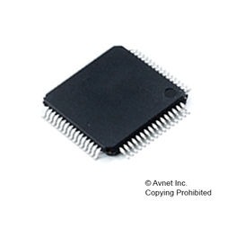
PIC18F6X8X devices are available in 64-pin TQFP and 68-pin PLCC packages. PIC18F8X8X devices are available in the 80-pin TQFP package. They are differentiated from each other in four ways: 1. Flash program memory (48 Kbytes for PIC18FX585 devices, 64 Kbytes for PIC18FX680) 2. A/D channels (12 for PIC18F6X8X devices, 16 for PIC18F8X8X) 3. I/O ports (7 on PIC18F6X8X devices, 9 on PIC18F8X8X) 4. External program memory interface (present only on PIC18F8X8X devices) All other features for devices in the PIC18F6585/8585/6680/8680 family are identical.
- High-Performance RISC CPU:
- Source code compatible with the PIC16 and PIC17 instruction sets
- Linear program memory addressing to 2 Mbytes
- Linear data memory addressing to 4096 bytes
- 1 Kbyte of data EEPROM
- Up to 10 MIPs operation: – DC – 40 MHz osc./clock input – 4 MHz-10 MHz osc./clock input with PLL active
- 16-bit wide instructions, 8-bit wide data path
- Priority levels for interrupts
- 31-level, software accessible hardware stack
- 8 x 8 Single-Cycle Hardware Multiplier
- High current sink/source 25 mA/25 mA
- Four external interrupt pins
- Timer0 module: 8-bit/16-bit timer/counter
- Timer1 module: 16-bit timer/counter
- Timer2 module: 8-bit timer/counter
- Timer3 module: 16-bit timer/counter
- Up to 16-channel, 10-bit Analog-to-Digital Converter module (A/D) with: – Fast sampling rate – Programmable acquisition time – Conversion available during Sleep
- Programmable 16-level Low-Voltage Detection (LVD) module: – Supports interrupt on Low-Voltage Detection
- Programmable Brown-out Reset (BOR)
- Dual analog comparators:- Programmable input/output configuration
- 100,000 erase/write cycle Enhanced Flash program memory typical
- 1,000,000 erase/write cycle Data EEPROM memory typical
- 1-second programming time
- Flash/Data EEPROM Retention: > 40 years
- Self-reprogrammable under software control
- Power-on Reset (POR), Power-up Timer (PWRT) and Oscillator Start-up Timer (OST)
- Watchdog Timer (WDT) with its own On-Chip RC Oscillator
- Programmable code protection
- Power saving Sleep mode
- Selectable oscillator options including: – Software enabled 4x Phase Lock Loop (of primary oscillator) – Secondary Oscillator (32 kHz) clock input
- In-Circuit Serial Programming™ (ICSP™) via two pins
MPLAB® In-Circuit Debug (ICD) via two pins