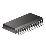
MCU 8-bit PIC18 PIC RISC 64KB Flash 2.5V/3.3V 28-Pin SOIC W Tube, PIC18LF26J13-I/SO, Microchip

PIC18LF26J13 incorporate a range of features that can significantly reduce power consumption during operation Alternate Run Modes: By clocking the controller from the Timer1 source or the internal RC oscillator, power consumption during code execution can be reduced by as much as 90%. Multiple Idle Modes: The controller can also run with its CPU core disabled but the peripherals still active. In these states, power consumption can be reduced even further, to as little as 4% of normal operational requirements. On-the-Fly Mode Switching: The power-managed modes are invoked by user code during operation, allowing the users to incorporate power-saving ideas into their application’s software design Deep Sleep: The 2.5V internal core voltage regulator on F parts can be shutdown to cut power consumption to as low as 15 nA (typical). Certain features can remain operating during Deep Sleep, such as the Real-Time Clock Calendar. Ultra Low Power Wake-Up: Waking from Sleep or Deep Sleep modes after a period of time can be done without an oscillator/clock source, saving All of the devices in the PIC18F47J13 family offer five different oscillator options, allowing users a range of choices in developing application hardware. These include: Two Crystal modes, using crystals or ceramic resonators. Two External Clock modes, offering the option of a divide-by-4 clock output. An internal oscillator block, which provides an 8 MHz clock and an INTRC source (approximately 31 kHz, stable over temperature and VDD), as well as a range of six user selectable clock frequencies, between 125 kHz to 4 MHz, for a total of eight clock frequencies. This option frees an oscillator pin for use as an additional general purpose I/O. A Phase Lock Loop (PLL) frequency multiplier available to the high-speed crystal, and external and internal oscillators, providing a clock speed up to 48 MHz The internal oscillator block provides a stable reference source that gives the PIC18F47J13 family additional features for robust operation Fail-Safe Clock Monitor: This option constantly monitors the main clock source against a reference signal provided by the internal oscillator. If a clock failure occurs, the controller is switched to the internal oscillator, allowing for continued low-speed operation or a safe application shutdown. Two-Speed Start-up: This option allows the internal oscillator to serve as the clock source from Power-on Reset (POR), or wake-up from Sleep mode, until the primary clock source is available

  • Power Management Features with nanoWatt XLP for Extreme Low Power:
  • Deep Sleep mode: CPU Off, Peripherals Off, SRAM Off, Currents Down to 9 nA and 700 nA with RTCC:
    • Able to wake-up on external triggers, programmable WDT or RTCC alarm
    • Ultra Low-Power Wake-up (ULPWU)
  • Sleep mode: CPU Off, Peripherals Off, SRAM On, Fast Wake-up, Currents Down to 0.2 µA, 2V Typical
  • Idle: CPU Off, SRAM On, Currents Down to 1.7 µA Typical
  • Run: CPU On, SRAM On, Currents Down to 5.8 µA Typical
  • Timer1 Oscillator w/RTCC: 0.7 µA, 32 kHz Typical
  • Watchdog Timer: 0.33 µA, 2V Typical Flexible Oscillator Structure:
  • Two External Clock modes, Up to 48 MHz (12 MIPS)
  • Integrated Crystal/Resonator Driver
  • Low-Power 31 kHz Internal RC Oscillator
  • Tunable Internal Oscillator (31 kHz to 8 MHz, ±0.15% Typical, ±1% Max.)
  • Precision 48 MHz PLL or 4x PLL Options
  • Low-Power Secondary Oscillator using Timer1 @ 32 kHz
  • Fail-Safe Clock Monitor (FSCM):
    • Allows for safe shutdown if any clock stops
  • Programmable Reference Clock Output Generator Peripheral Highlights:
  • Peripheral Pin Select:
    • Allows independent I/O mapping of many peripherals
    • Continuous hardware integrity checking and safety interlocks prevent unintentional configuration changes
  • Hardware Real-Time Clock/Calendar (RTCC):
    • Provides clock, calendar and alarm functions
  • High-Current Sink/Source 25 mA/25mA (PORTB and PORTC)
  • Four Programmable External Interrupts
  • Four Input Change Interrupts
  • Three Enhanced Capture/Compare/PWM (ECCP) modules:
    • One, two or four PWM outputs
    • Selectable polarity
    • Programmable dead time
    • Auto-shutdown and auto-restart
    • Pulse steering control Peripheral Highlights (cont.):
  • Seven Capture/Compare/PWM (CCP) modules
  • Two Master Synchronous Serial Port (MSSP) modules featuring:
    • 3-wire SPI (all 4 modes)
    • SPI Direct Memory Access (DMA) channel w/1024 byte count
    • I2C™ Master and Slave modes
  • 8-Bit Parallel Master Port/Enhanced Parallel Slave Port
  • Three Analog Comparators with Input Multiplexing
  • 12-Bit Analog-to-Digital (A/D) Converter module:
    • Up to 13 input channels
    • Auto-acquisition capability
    • 10-bit mode for 100 ksps conversion speed
    • Conversion available during Sleep
  • High/Low-Voltage Detect module
  • Charge Time Measurement Unit (CTMU):
    • Provides a precise resolution time measurement for both flow measurement and simple temperature sensing
    • Supports capacitive touch sensing for touch screens and capacitive switches
  • Two Enhanced USART modules:
    • Supports RS-485, RS-232 and LIN/J2602
    • Auto-wake-up on Start bit
    • Auto-Baud Detect (ABD) Special Microcontroller Features:
  • 5.5V Tolerant Inputs (digital only pins)
  • Low-Power, High-Speed CMOS Flash Technology
  • C Compiler Optimized Architecture for Re-Entrant Code
  • Priority Levels for Interrupts
  • Self-Programmable under Software Control
  • 8 x 8 Single-Cycle Hardware Multiplier
  • Extended Watchdog Timer (WDT):
    • Programmable period from 4 ms to 131s

Характеристики

Analog_comparators

3

Operating_supply_voltage

2.5, 3.3 V

Max_power_dissipation

1000 mW

Min_operating_supply_voltage

2 V

Max_operating_supply_voltage

2.75, 3.6 V

Watchdog

1

Supplier_package

SOIC W

Specifications

https://4donline.ihs.com/images/VipMasterIC/IC/MCHP/MCHP-S-A0002954618/MCHP-S-A0002954618-1.pdf?hkey=52A5661711E402568146F3353EA87419

Screening_level

Industrial

Schedule_b

8542310000

Ram_size

3760 byte

Program_memory_type

Flash

Program_memory_size

64 KB

Product_dimensions

17.9 x 7.5 x 2.35 mm

Pin_count

28

Operating_temperature

-40 to 85 °C

On_chip_adc

10-chx12-bit

Бренд

Number_of_timers

8

Number_of_programmable_i_os

3

Msl_level

1, 3

Mounting

Surface Mount

Maximum_speed

48 MHz

Max_processing_temp

260

Lead_finish

Matte Tin

Тип интерфейса

I2C/SPI/USART

Instruction_set_architecture

RISC

Htsn

8542310001

Eccn

3A991.A.2

Device_core

PIC

Data_bus_width

8 Bit

Country_of_origin

China

Max_expanded_memory_size

2 MB

SKU: PIC18LF26J13-I/SO

Description

PIC18LF26J13 incorporate a range of features that can significantly reduce power consumption during operation Alternate Run Modes: By clocking the controller from the Timer1 source or the internal RC oscillator, power consumption during code execution can be reduced by as much as 90%. Multiple Idle Modes: The controller can also run with its CPU core disabled but the peripherals still active. In these states, power consumption can be reduced even further, to as little as 4% of normal operational requirements. On-the-Fly Mode Switching: The power-managed modes are invoked by user code during operation, allowing the users to incorporate power-saving ideas into their application’s software design Deep Sleep: The 2.5V internal core voltage regulator on F parts can be shutdown to cut power consumption to as low as 15 nA (typical). Certain features can remain operating during Deep Sleep, such as the Real-Time Clock Calendar. Ultra Low Power Wake-Up: Waking from Sleep or Deep Sleep modes after a period of time can be done without an oscillator/clock source, saving All of the devices in the PIC18F47J13 family offer five different oscillator options, allowing users a range of choices in developing application hardware. These include: Two Crystal modes, using crystals or ceramic resonators. Two External Clock modes, offering the option of a divide-by-4 clock output. An internal oscillator block, which provides an 8 MHz clock and an INTRC source (approximately 31 kHz, stable over temperature and VDD), as well as a range of six user selectable clock frequencies, between 125 kHz to 4 MHz, for a total of eight clock frequencies. This option frees an oscillator pin for use as an additional general purpose I/O. A Phase Lock Loop (PLL) frequency multiplier available to the high-speed crystal, and external and internal oscillators, providing a clock speed up to 48 MHz The internal oscillator block provides a stable reference source that gives the PIC18F47J13 family additional features for robust operation Fail-Safe Clock Monitor: This option constantly monitors the main clock source against a reference signal provided by the internal oscillator. If a clock failure occurs, the controller is switched to the internal oscillator, allowing for continued low-speed operation or a safe application shutdown. Two-Speed Start-up: This option allows the internal oscillator to serve as the clock source from Power-on Reset (POR), or wake-up from Sleep mode, until the primary clock source is available

  • Power Management Features with nanoWatt XLP for Extreme Low Power:
  • Deep Sleep mode: CPU Off, Peripherals Off, SRAM Off, Currents Down to 9 nA and 700 nA with RTCC:
    • Able to wake-up on external triggers, programmable WDT or RTCC alarm
    • Ultra Low-Power Wake-up (ULPWU)
  • Sleep mode: CPU Off, Peripherals Off, SRAM On, Fast Wake-up, Currents Down to 0.2 µA, 2V Typical
  • Idle: CPU Off, SRAM On, Currents Down to 1.7 µA Typical
  • Run: CPU On, SRAM On, Currents Down to 5.8 µA Typical
  • Timer1 Oscillator w/RTCC: 0.7 µA, 32 kHz Typical
  • Watchdog Timer: 0.33 µA, 2V Typical Flexible Oscillator Structure:
  • Two External Clock modes, Up to 48 MHz (12 MIPS)
  • Integrated Crystal/Resonator Driver
  • Low-Power 31 kHz Internal RC Oscillator
  • Tunable Internal Oscillator (31 kHz to 8 MHz, ±0.15% Typical, ±1% Max.)
  • Precision 48 MHz PLL or 4x PLL Options
  • Low-Power Secondary Oscillator using Timer1 @ 32 kHz
  • Fail-Safe Clock Monitor (FSCM):
    • Allows for safe shutdown if any clock stops
  • Programmable Reference Clock Output Generator Peripheral Highlights:
  • Peripheral Pin Select:
    • Allows independent I/O mapping of many peripherals
    • Continuous hardware integrity checking and safety interlocks prevent unintentional configuration changes
  • Hardware Real-Time Clock/Calendar (RTCC):
    • Provides clock, calendar and alarm functions
  • High-Current Sink/Source 25 mA/25mA (PORTB and PORTC)
  • Four Programmable External Interrupts
  • Four Input Change Interrupts
  • Three Enhanced Capture/Compare/PWM (ECCP) modules:
    • One, two or four PWM outputs
    • Selectable polarity
    • Programmable dead time
    • Auto-shutdown and auto-restart
    • Pulse steering control Peripheral Highlights (cont.):
  • Seven Capture/Compare/PWM (CCP) modules
  • Two Master Synchronous Serial Port (MSSP) modules featuring:
    • 3-wire SPI (all 4 modes)
    • SPI Direct Memory Access (DMA) channel w/1024 byte count
    • I2C™ Master and Slave modes
  • 8-Bit Parallel Master Port/Enhanced Parallel Slave Port
  • Three Analog Comparators with Input Multiplexing
  • 12-Bit Analog-to-Digital (A/D) Converter module:
    • Up to 13 input channels
    • Auto-acquisition capability
    • 10-bit mode for 100 ksps conversion speed
    • Conversion available during Sleep
  • High/Low-Voltage Detect module
  • Charge Time Measurement Unit (CTMU):
    • Provides a precise resolution time measurement for both flow measurement and simple temperature sensing
    • Supports capacitive touch sensing for touch screens and capacitive switches
  • Two Enhanced USART modules:
    • Supports RS-485, RS-232 and LIN/J2602
    • Auto-wake-up on Start bit
    • Auto-Baud Detect (ABD) Special Microcontroller Features:
  • 5.5V Tolerant Inputs (digital only pins)
  • Low-Power, High-Speed CMOS Flash Technology
  • C Compiler Optimized Architecture for Re-Entrant Code
  • Priority Levels for Interrupts
  • Self-Programmable under Software Control
  • 8 x 8 Single-Cycle Hardware Multiplier
  • Extended Watchdog Timer (WDT):
    • Programmable period from 4 ms to 131s

Additional information

Analog_comparators

3

Operating_supply_voltage

2.5, 3.3 V

Max_power_dissipation

1000 mW

Min_operating_supply_voltage

2 V

Max_operating_supply_voltage

2.75, 3.6 V

Watchdog

1

Supplier_package

SOIC W

Specifications

https://4donline.ihs.com/images/VipMasterIC/IC/MCHP/MCHP-S-A0002954618/MCHP-S-A0002954618-1.pdf?hkey=52A5661711E402568146F3353EA87419

Screening_level

Industrial

Schedule_b

8542310000

Ram_size

3760 byte

Program_memory_type

Flash

Program_memory_size

64 KB

Product_dimensions

17.9 x 7.5 x 2.35 mm

Pin_count

28

Operating_temperature

-40 to 85 °C

On_chip_adc

10-chx12-bit

Бренд

Number_of_timers

8

Number_of_programmable_i_os

3

Msl_level

1, 3

Mounting

Surface Mount

Maximum_speed

48 MHz

Max_processing_temp

260

Lead_finish

Matte Tin

Тип интерфейса

I2C/SPI/USART

Instruction_set_architecture

RISC

Htsn

8542310001

Eccn

3A991.A.2

Device_core

PIC

Data_bus_width

8 Bit

Country_of_origin

China

Max_expanded_memory_size

2 MB