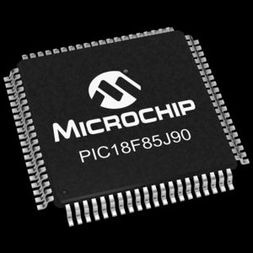
MCU 8-bit PIC18 PIC RISC 32KB Flash 2.5V/3.3V 80-Pin TQFP Tray, PIC18F85J90-I/PT, Microchip

PIC18F85J90 combines the traditional advantages of all PIC18 microcontrollers – namely, high computational performance and a rich feature set – with a versatile on-chip LCD driver, while maintaining an extremely competitive price point. These features make the PIC18F85J90 family a logical choice for many high-performance applications where price is a primary consideration. All of the devices in the PIC18F85J90 family incorporate a range of features that can significantly reduce power consumption during operation Alternate Run Modes: By clocking the controller from the Timer1 source or the internal RC oscillator, power consumption during code execution can be reduced by as much as 90%. Multiple Idle Modes: The controller can also run with its CPU core disabled but the peripherals still active. In these states, power consumption can be reduced even further, to as little as 4% of normal operation requirements On-the-Fly Mode Switching: The power-managed modes are invoked by user code during operation, allowing the user to incorporate power-saving ideas into their application’s software design. All of the devices in the PIC18F85J90 family offer six different oscillator options, allowing users a range of choices in developing application hardware. These include: Two Crystal modes, using crystals or ceramic resonators. Two External Clock modes, offering the option of a divide-by-4 clock output. A Phase Lock Loop (PLL) frequency multiplier, available to the External Oscillator modes which allows clock speeds of up to 40 MHz. An internal oscillator block which provides an 8 MHz clock (±2% accuracy) and an INTRC source (approximately 31 kHz, stable over temperature and VDD), as well as a range of six user-selectable clock frequencies, between 125 kHz to 4 MHz, for a total of eight clock frequencies. This option frees the two oscillator pins for use as additional general purpose I/O The internal oscillator block provides a stable reference source that gives the family additional features for robust operation: Fail-Safe Clock Monitor: This option constantly monitors the main clock source against a reference signal provided by the internal oscillator. If a clock failure occurs, the controller is switched to the internal oscillator, allowing for continued low-speed operation or a safe application shutdown. Two-Speed Start-up: This option allows the internal oscillator to serve as the clock source from Power-on Reset, or wake-up from Sleep mode, until the primary clock source is available.

  • Low-Power Features:
  • Power-Managed modes: Run, Idle, Sleep
  • Run current down to 7 µA, typical
  • Idle current down to 2.5 µA, typical
  • Sleep current down to 100 nA, typical
  • Fast INTOSC start-up from Sleep, 1 µs typical
  • Two-Speed Oscillator Start-up reduces crystal stabilization wait time LCD Driver Module Features:
  • Direct LCD Panel Drive Capability: – Can drive LCD panel while in Sleep mode
  • Up to 48 Segments and 192 Pixels; Software Selectable
  • Programmable LCD Timing module: – Multiple LCD timing sources available – Up to 4 commons: static, 1/2, 1/3 or 1/4 multiplex – Static, 1/2 or 1/3 Bias configuration
  • Integrated Charge Pump Module with Voltage Boost Special Microcontroller Features:
  • 1000 Erase/Write Cycle Flash Program Memory, Typical
  • Flash Retention: 20 Years Minimum
  • Self-Programmable under Software Control
  • Priority Levels for Interrupts
  • 8 x 8 Single-Cycle Hardware Multiplier
  • Extended Watchdog Timer (WDT): – Programmable period from 4 ms to 131s
  • In-Circuit Serial Programming™ (ICSP™) via Two Pins
  • In-Circuit Debug with 3 Breakpoints via Two Pins
  • Operating Voltage Range: 2.0V to 3.6V
  • On-Chip 2.5V Regulator Flexible Oscillator Structure:
  • Two Crystal modes, 4-25 MHz
  • Two External Clock modes, up to 40 MHz
  • Internal Oscillator Block: – 8 user-selectable frequencies from 31.25 kHz to 8 MHz
  • Secondary Oscillator using Timer1 @ 32 kHz
  • Fail-Safe Clock Monitor: – Allows for safe shutdown if peripheral clock fails
  • Peripheral Highlights:
  • High-Current Sink/Source: 25 mA/25 mA (PORTB and PORTC)
  • Sleep Current as Low as 100 nA
  • Up to Four External Interrupts
  • Four 8-Bit/16-Bit Timer/Counter modules: – Uses Timer1
  • Two Capture/Compare/PWM (CCP) modules: – Capture is 16-bit, max. resolution 6.25 ns (TCY/16) – Compare is 16-bit, max. resolution 100 ns (TCY) – PWM output: PWM resolution is up to 10-bit
  • Master Synchronous Serial Port (MSSP) module with Two Modes of Operation: – 3-wire/4-wire SPI (supports all 4 SPI modes) – I2C™ Master and Slave modes
  • One Addressable USART module
  • One Enhanced USART module: – Supports LIN/J2602 – Auto-wake-up on Start bit and Break character – Auto-Baud Detect
  • 10-Bit, up to 12-Channel A/D Converter: – Auto-acquisition – Conversion available during Sleep
  • Two Analog Comparators
  • Programmable Reference Voltage for Comparators

Характеристики

Бренд

Number_of_programmable_i_os

67

Screening_level

Industrial

Schedule_b

8542310000

Program_memory_type

Flash

Product_dimensions

12 x 12 x 1 mm

Pin_count

80

Operating_temperature

-40 to 85 °C

Operating_supply_voltage

2.5, 3.3 V

On_chip_adc

12-chx10-bit

Number_of_timers

4

Msl_level

1, 3

Country_of_origin

China

Mounting

Surface Mount

Maximum_speed

40 MHz

Lead_finish

Matte Tin

Тип интерфейса

I2C/SPI/USART

Instruction_set_architecture

RISC

Htsn

8542310001

Eccn

3A991.A.2

Device_core

PIC

Data_bus_width

8 Bit

Specifications

https://4donline.ihs.com/images/VipMasterIC/IC/MCHP/MCHPS03086/MCHPS03086-1.pdf?hkey=52A5661711E402568146F3353EA87419

SKU: PIC18F85J90-I/PT

Description

PIC18F85J90 combines the traditional advantages of all PIC18 microcontrollers – namely, high computational performance and a rich feature set – with a versatile on-chip LCD driver, while maintaining an extremely competitive price point. These features make the PIC18F85J90 family a logical choice for many high-performance applications where price is a primary consideration. All of the devices in the PIC18F85J90 family incorporate a range of features that can significantly reduce power consumption during operation Alternate Run Modes: By clocking the controller from the Timer1 source or the internal RC oscillator, power consumption during code execution can be reduced by as much as 90%. Multiple Idle Modes: The controller can also run with its CPU core disabled but the peripherals still active. In these states, power consumption can be reduced even further, to as little as 4% of normal operation requirements On-the-Fly Mode Switching: The power-managed modes are invoked by user code during operation, allowing the user to incorporate power-saving ideas into their application’s software design. All of the devices in the PIC18F85J90 family offer six different oscillator options, allowing users a range of choices in developing application hardware. These include: Two Crystal modes, using crystals or ceramic resonators. Two External Clock modes, offering the option of a divide-by-4 clock output. A Phase Lock Loop (PLL) frequency multiplier, available to the External Oscillator modes which allows clock speeds of up to 40 MHz. An internal oscillator block which provides an 8 MHz clock (±2% accuracy) and an INTRC source (approximately 31 kHz, stable over temperature and VDD), as well as a range of six user-selectable clock frequencies, between 125 kHz to 4 MHz, for a total of eight clock frequencies. This option frees the two oscillator pins for use as additional general purpose I/O The internal oscillator block provides a stable reference source that gives the family additional features for robust operation: Fail-Safe Clock Monitor: This option constantly monitors the main clock source against a reference signal provided by the internal oscillator. If a clock failure occurs, the controller is switched to the internal oscillator, allowing for continued low-speed operation or a safe application shutdown. Two-Speed Start-up: This option allows the internal oscillator to serve as the clock source from Power-on Reset, or wake-up from Sleep mode, until the primary clock source is available.

  • Low-Power Features:
  • Power-Managed modes: Run, Idle, Sleep
  • Run current down to 7 µA, typical
  • Idle current down to 2.5 µA, typical
  • Sleep current down to 100 nA, typical
  • Fast INTOSC start-up from Sleep, 1 µs typical
  • Two-Speed Oscillator Start-up reduces crystal stabilization wait time LCD Driver Module Features:
  • Direct LCD Panel Drive Capability: – Can drive LCD panel while in Sleep mode
  • Up to 48 Segments and 192 Pixels; Software Selectable
  • Programmable LCD Timing module: – Multiple LCD timing sources available – Up to 4 commons: static, 1/2, 1/3 or 1/4 multiplex – Static, 1/2 or 1/3 Bias configuration
  • Integrated Charge Pump Module with Voltage Boost Special Microcontroller Features:
  • 1000 Erase/Write Cycle Flash Program Memory, Typical
  • Flash Retention: 20 Years Minimum
  • Self-Programmable under Software Control
  • Priority Levels for Interrupts
  • 8 x 8 Single-Cycle Hardware Multiplier
  • Extended Watchdog Timer (WDT): – Programmable period from 4 ms to 131s
  • In-Circuit Serial Programming™ (ICSP™) via Two Pins
  • In-Circuit Debug with 3 Breakpoints via Two Pins
  • Operating Voltage Range: 2.0V to 3.6V
  • On-Chip 2.5V Regulator Flexible Oscillator Structure:
  • Two Crystal modes, 4-25 MHz
  • Two External Clock modes, up to 40 MHz
  • Internal Oscillator Block: – 8 user-selectable frequencies from 31.25 kHz to 8 MHz
  • Secondary Oscillator using Timer1 @ 32 kHz
  • Fail-Safe Clock Monitor: – Allows for safe shutdown if peripheral clock fails
  • Peripheral Highlights:
  • High-Current Sink/Source: 25 mA/25 mA (PORTB and PORTC)
  • Sleep Current as Low as 100 nA
  • Up to Four External Interrupts
  • Four 8-Bit/16-Bit Timer/Counter modules: – Uses Timer1
  • Two Capture/Compare/PWM (CCP) modules: – Capture is 16-bit, max. resolution 6.25 ns (TCY/16) – Compare is 16-bit, max. resolution 100 ns (TCY) – PWM output: PWM resolution is up to 10-bit
  • Master Synchronous Serial Port (MSSP) module with Two Modes of Operation: – 3-wire/4-wire SPI (supports all 4 SPI modes) – I2C™ Master and Slave modes
  • One Addressable USART module
  • One Enhanced USART module: – Supports LIN/J2602 – Auto-wake-up on Start bit and Break character – Auto-Baud Detect
  • 10-Bit, up to 12-Channel A/D Converter: – Auto-acquisition – Conversion available during Sleep
  • Two Analog Comparators
  • Programmable Reference Voltage for Comparators

Additional information

Бренд

Number_of_programmable_i_os

67

Screening_level

Industrial

Schedule_b

8542310000

Program_memory_type

Flash

Product_dimensions

12 x 12 x 1 mm

Pin_count

80

Operating_temperature

-40 to 85 °C

Operating_supply_voltage

2.5, 3.3 V

On_chip_adc

12-chx10-bit

Number_of_timers

4

Msl_level

1, 3

Country_of_origin

China

Mounting

Surface Mount

Maximum_speed

40 MHz

Lead_finish

Matte Tin

Тип интерфейса

I2C/SPI/USART

Instruction_set_architecture

RISC

Htsn

8542310001

Eccn

3A991.A.2

Device_core

PIC

Data_bus_width

8 Bit

Specifications

https://4donline.ihs.com/images/VipMasterIC/IC/MCHP/MCHPS03086/MCHPS03086-1.pdf?hkey=52A5661711E402568146F3353EA87419