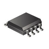
MCU 8-bit PIC12 PIC RISC 1.75KB Flash 8-Pin SOIC N Tube, PIC12HV752-I/SN, Microchip

Program Memory Organization The PIC12F752/HV752 has a 13-bit program counter capable of addressing an 8K x 14 program memory space. Only the first 1K x 14 (0000h-03FFh) is physically implemented. Accessing a location above these boundaries will cause a wrap-around within the first 1K x 14 space for PIC12F752/HV752. The Reset vector is at 0000h and the interrupt vector is at 0004h 2.2 Data Memory Organization The data memory is partitioned into four banks, which contain the General Purpose Registers (GPR) and the Special Function Registers (SFR). The Special Function Registers are located in the first 32 locations of each bank. Register locations 40h-6Fh in Bank 0 are General Purpose Registers, implemented as static RAM. Register locations 70h-7Fh in Bank 0 are Common RAM and shared as the last 16 addresses in all Banks. All other RAM is unimplemented and returns ‘0’ when read. The RP<1:0> bits of the STATUS register are the bank select bits. RP1 RP0 0 0 ? Bank 0 is selected 0 1 ? Bank 1 is selected 1 0 ? Bank 2 is selected 1 1 ? Bank 3 is selected

  • High-Performance RISC CPU:
  • Only 35 Instructions to Learn:
    • All single-cycle instructions except branches
  • Operating Speed:
    • DC – 20 MHz clock input
    • DC – 200 ns instruction cycle
  • 1024 x 14 On-chip Flash Program Memory
  • Self Read/Write Program Memory
  • 64 x 8 General Purpose Registers (SRAM)
  • Interrupt Capability
  • 8-Level Deep Hardware Stack
  • Direct, Indirect and Relative Addressing modes
  • Microcontroller Features:
  • Precision Internal Oscillator:
    • Factory calibrated to ±1%, typical
    • Software selectable frequency: 8 MHz, 4 MHz, 1 MHz or 31 kHz
    • Software tunable
  • Power-Saving Sleep mode
  • Voltage Range (PIC12F752):
    • 2.0V to 5.5V
  • Shunt Voltage Regulator (PIC12HV752)
    • 2.0V to user defined
    • 5-volt regulation
    • 1 mA to 50 mA shunt range
  • Multiplexed Master Clear with Pull-up/Input Pin
  • Interrupt-on-Change Pins
  • Individually Programmable Weak Pull-ups
  • Power-on Reset (POR)
  • Power-up Timer (PWRT)
  • Brown-out Reset (BOR)
  • Watchdog Timer (WDT) with Internal Oscillator for Reliable Operation
  • Industrial and Extended Temperature Range
  • High Endurance Flash:
    • 100,000 write Flash endurance
    • Flash retention: >40 years
  • Programmable Code Protection
  • In-Circuit Debug (ICD) via Two Pins
  • In-Circuit Serial Programming™ (ICSP™) via Two Pins
  • Low-Power Features:
  • Standby Current:
    • 50 nA @ 2.0V, typical
  • Operating Current:
    • 11 uA @ 32 kHz, 2.0V, typical
    • 260 uA @ 4 MHz, 2.0V, typical
  • Watchdog Timer Current:
  • <1 uA @ 2.0V, typical
  • Peripheral Features:
  • Five I/O Pins and One Input-only Pin
  • High Current Source/Sink:
    • 50 mA I/O, (2 pins)
    • 25 mA I/O, (3 pins)
  • Two High-Speed Analog Comparator modules:
    • 40 ns response time
    • Fixed Voltage Reference (FVR)
    • Programmable on-chip voltage reference via integrated 5-bit DAC
    • Internal/external inputs and outputs (selectable)
    • Built-in Hysteresis (software selectable)
  • A/D Converter:
    • 10-bit resolution
    • Four external channels
    • Two internal reference voltage channels
  • Dual Range Digital-to-Analog Converter (DAC):
    • 5-bit resolution
    • Full Range or Limited Range output
    • 4 mV steps @ 2.0V (Limited Range)
    • 65 mV steps @ 2.0V (Full Range)
  • Fixed Voltage Reference (FVR), 1.2V reference
  • Capture, Compare, PWM (CCP) module:
    • 16-bit Capture, max. resolution = 12.5 ns
    • Compare, max. resolution = 200 ns
    • 10-bit PWM, max. frequency = 20 kHz
  • Timer0: 8-Bit Timer/Counter with 8-Bit Prescaler
  • Enhanced Timer1:
    • 16-bit Timer/Counter with Prescaler
    • External Timer1 Gate (count enable)
    • Four Selectable Clock sources
  • Timer2: 8-Bit Timer/Counter with Prescaler:
    • 8-bit Period Register and Postscaler
  • Hardware Limit Timer (HLT):
    • 8-bit Timer with Prescaler
    • 8-bit period register and postscaler
    • Asynchronous H/W Reset sources
  • Complementary Output Generator (COG):
    • Complementary Waveforms from selectable sources
    • Two I/O (50 mA) for direct MOSFET drive
    • Rising and/or Falling edge dead-band control
    • Phase control, Blanking control
    • Auto-shutdown

Характеристики

Analog_comparators

2

Operating_temperature

-40 to 85 °C

Min_operating_supply_voltage

4.5 V

Max_operating_supply_voltage

5 V

Watchdog

1

Supplier_package

SOIC N

Specifications

https://4donline.ihs.com/images/VipMasterIC/IC/MCHP/MCHP-S-A0001211420/MCHP-S-A0001211420-1.pdf?hkey=52A5661711E402568146F3353EA87419

Screening_level

Industrial

Schedule_b

8542310000

Ram_size

64 byte

Program_memory_type

Flash

Program_memory_size

1.75 KB

Product_dimensions

4.9 x 3.9 x 1.25 mm

Pin_count

8

On_chip_adc

4-chx10-bit

Бренд

Number_of_timers

4

Number_of_programmable_i_os

6

Msl_level

1, 3

Mounting

Surface Mount

Maximum_speed

20 MHz

Max_processing_temp

260

Lead_finish

Matte Tin

Instruction_set_architecture

RISC

Htsn

8542310001

Eccn

EAR99

Device_core

PIC

Data_bus_width

8 Bit

Country_of_origin

China

Max_power_dissipation

800 mW

Артикул: PIC12HV752-I/SN

Описание

Program Memory Organization The PIC12F752/HV752 has a 13-bit program counter capable of addressing an 8K x 14 program memory space. Only the first 1K x 14 (0000h-03FFh) is physically implemented. Accessing a location above these boundaries will cause a wrap-around within the first 1K x 14 space for PIC12F752/HV752. The Reset vector is at 0000h and the interrupt vector is at 0004h 2.2 Data Memory Organization The data memory is partitioned into four banks, which contain the General Purpose Registers (GPR) and the Special Function Registers (SFR). The Special Function Registers are located in the first 32 locations of each bank. Register locations 40h-6Fh in Bank 0 are General Purpose Registers, implemented as static RAM. Register locations 70h-7Fh in Bank 0 are Common RAM and shared as the last 16 addresses in all Banks. All other RAM is unimplemented and returns ‘0’ when read. The RP<1:0> bits of the STATUS register are the bank select bits. RP1 RP0 0 0 ? Bank 0 is selected 0 1 ? Bank 1 is selected 1 0 ? Bank 2 is selected 1 1 ? Bank 3 is selected

  • High-Performance RISC CPU:
  • Only 35 Instructions to Learn:
    • All single-cycle instructions except branches
  • Operating Speed:
    • DC – 20 MHz clock input
    • DC – 200 ns instruction cycle
  • 1024 x 14 On-chip Flash Program Memory
  • Self Read/Write Program Memory
  • 64 x 8 General Purpose Registers (SRAM)
  • Interrupt Capability
  • 8-Level Deep Hardware Stack
  • Direct, Indirect and Relative Addressing modes
  • Microcontroller Features:
  • Precision Internal Oscillator:
    • Factory calibrated to ±1%, typical
    • Software selectable frequency: 8 MHz, 4 MHz, 1 MHz or 31 kHz
    • Software tunable
  • Power-Saving Sleep mode
  • Voltage Range (PIC12F752):
    • 2.0V to 5.5V
  • Shunt Voltage Regulator (PIC12HV752)
    • 2.0V to user defined
    • 5-volt regulation
    • 1 mA to 50 mA shunt range
  • Multiplexed Master Clear with Pull-up/Input Pin
  • Interrupt-on-Change Pins
  • Individually Programmable Weak Pull-ups
  • Power-on Reset (POR)
  • Power-up Timer (PWRT)
  • Brown-out Reset (BOR)
  • Watchdog Timer (WDT) with Internal Oscillator for Reliable Operation
  • Industrial and Extended Temperature Range
  • High Endurance Flash:
    • 100,000 write Flash endurance
    • Flash retention: >40 years
  • Programmable Code Protection
  • In-Circuit Debug (ICD) via Two Pins
  • In-Circuit Serial Programming™ (ICSP™) via Two Pins
  • Low-Power Features:
  • Standby Current:
    • 50 nA @ 2.0V, typical
  • Operating Current:
    • 11 uA @ 32 kHz, 2.0V, typical
    • 260 uA @ 4 MHz, 2.0V, typical
  • Watchdog Timer Current:
  • <1 uA @ 2.0V, typical
  • Peripheral Features:
  • Five I/O Pins and One Input-only Pin
  • High Current Source/Sink:
    • 50 mA I/O, (2 pins)
    • 25 mA I/O, (3 pins)
  • Two High-Speed Analog Comparator modules:
    • 40 ns response time
    • Fixed Voltage Reference (FVR)
    • Programmable on-chip voltage reference via integrated 5-bit DAC
    • Internal/external inputs and outputs (selectable)
    • Built-in Hysteresis (software selectable)
  • A/D Converter:
    • 10-bit resolution
    • Four external channels
    • Two internal reference voltage channels
  • Dual Range Digital-to-Analog Converter (DAC):
    • 5-bit resolution
    • Full Range or Limited Range output
    • 4 mV steps @ 2.0V (Limited Range)
    • 65 mV steps @ 2.0V (Full Range)
  • Fixed Voltage Reference (FVR), 1.2V reference
  • Capture, Compare, PWM (CCP) module:
    • 16-bit Capture, max. resolution = 12.5 ns
    • Compare, max. resolution = 200 ns
    • 10-bit PWM, max. frequency = 20 kHz
  • Timer0: 8-Bit Timer/Counter with 8-Bit Prescaler
  • Enhanced Timer1:
    • 16-bit Timer/Counter with Prescaler
    • External Timer1 Gate (count enable)
    • Four Selectable Clock sources
  • Timer2: 8-Bit Timer/Counter with Prescaler:
    • 8-bit Period Register and Postscaler
  • Hardware Limit Timer (HLT):
    • 8-bit Timer with Prescaler
    • 8-bit period register and postscaler
    • Asynchronous H/W Reset sources
  • Complementary Output Generator (COG):
    • Complementary Waveforms from selectable sources
    • Two I/O (50 mA) for direct MOSFET drive
    • Rising and/or Falling edge dead-band control
    • Phase control, Blanking control
    • Auto-shutdown

Детали

Analog_comparators

2

Operating_temperature

-40 to 85 °C

Min_operating_supply_voltage

4.5 V

Max_operating_supply_voltage

5 V

Watchdog

1

Supplier_package

SOIC N

Specifications

https://4donline.ihs.com/images/VipMasterIC/IC/MCHP/MCHP-S-A0001211420/MCHP-S-A0001211420-1.pdf?hkey=52A5661711E402568146F3353EA87419

Screening_level

Industrial

Schedule_b

8542310000

Ram_size

64 byte

Program_memory_type

Flash

Program_memory_size

1.75 KB

Product_dimensions

4.9 x 3.9 x 1.25 mm

Pin_count

8

On_chip_adc

4-chx10-bit

Бренд

Number_of_timers

4

Number_of_programmable_i_os

6

Msl_level

1, 3

Mounting

Surface Mount

Maximum_speed

20 MHz

Max_processing_temp

260

Lead_finish

Matte Tin

Instruction_set_architecture

RISC

Htsn

8542310001

Eccn

EAR99

Device_core

PIC

Data_bus_width

8 Bit

Country_of_origin

China

Max_power_dissipation

800 mW