Описание
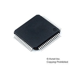
The MSC1210Yx is a completely integrated family of mixed-signal devices incorporating a high-resolution delta-sigma ADC, 8-channel multiplexer, burnout current sources, selectable buffered input, offset DAC (digital-to-analog converter), PGA (programmable gain amplifier), temperature sensor, voltage reference, 8-bit microcontroller, Flash Program Memory, Flash Data Memory, and Data SRAM, as shown in Figure 8. On-chip peripherals include an additional 32-bit accumulator, an SPI compatible serial port, dual USARTs, multiple digital input/output ports, watchdog timer, low-voltage detect, on-chip power-on reset, 16-bit PWM, and system timers, brownout reset, and three timer/counters. The microcontroller core is 8051 instruction set compatible. The microcontroller core is an optimized 8051 core that executes up to three times faster than the standard 8051 core, given the same clock source. That makes it possible to run the device at a lower external clock frequency and achieve the same performance at lower power than the standard 8051 core. The MSC1210Yx allows the user to uniquely configure the Flash and SRAM memory maps to meet the needs of their application. The Flash is programmable down to 2.7V using both serial and parallel programming methods. The Flash endurance is 1 million Erase/Write cycles. In addition, 1280 bytes of RAM are incorporated on-chip. The part has separate analog and digital supplies, which can be independently powered from 2.7V to +5.25V. At +3V operation, the power dissipation for the part is typically less than 4mW. The MSC1210Yx is packaged in a TQFP-64 package. The MSC1210Yx is designed for high-resolution measurement applications in smart transmitters, industrial process control, weigh scales, chromatography, and portable instrumentation.
- 24 Bits No Missing Codes
- 22 Bits Effective Resolution at 10Hz
- Low Noise: 75nV
- PGA From 1 to 128
- Precision On-Chip Voltage Reference
- 8 Differential/Single-Ended Channels
- On-Chip Offset/Gain Calibration
- Offset Drift: 0.1ppm/°C
- Gain Drift: 0.5ppm/°C
- On-Chip Temperature Sensor
- Burnout Sensor Detection
- Single-Cycle Conversion
- Selectable Buffer Input
- Microcontroller Core
- 8051-Compatible
- High-Speed Core
- 4 Clocks per Instruction Cycle
- DC to 33MHz
- Single Instruction 121ns
- Dual Data Pointer
- Memory
- Up To 32kB Flash Memory
- Flash Memory Partitioning
- Endurance 1M Erase/Write Cycles, 100 Year Data Retention
- In-System Serially Programmable
- External Program/Data Memory (64kB)
- 1,280 Bytes Data SRAM
- Flash Memory Security
- 2kB Boot ROM
- Programmable Wait State Control
- Peripheral Features
- 34 I/O Pins
- Additional 32-Bit Accumulator
- Three 16-Bit Timer/Counters
- System Timers
- Programmable Watchdog Timer
- Full-Duplex Dual USARTs
- Master/Slave SPI™
- 16-Bit PWM
- Power Management Control
- Idle Mode Current < 1mA
- Stop Mode Current < 1µA
- Programmable Brownout Reset
- Programmable Low Voltage Detect
- 24 Interrupt Sources
- Two Hardware Breakpoints
- Pin-Compatible with MSC1211/12/13/14
- Package: TQFP-64
- Low Power: 4mW
- Industrial Temperature Range: –40°C to +125°C
- Power Supply: 2.7V to 5.25V
- Industrial Process Control
- Instrumentation
- Liquid/Gas Chromatography
- Blood Analysis
- Smart Transmitters
- Portable Instruments
- Weigh Scales
- Pressure Transducers
- Intelligent Sensors
- Portable Applications
- DAS Systems