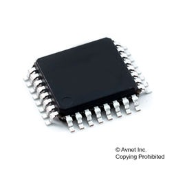
MCU 8-Bit ML610100 nX-U8/100 RISC 32KB Flash 3.3V/5V 32-Pin LQFP, ML610Q112-NNNTCZ07FL, ROHM

This LSI is a high-performance 8-bit CMOS microcontroller into which rich peripheral circuits, such as timers, PWM, UART, I2 C bus interface (master/slave), synchronous serial port, voltage level supervisor analog comparators and 10-bit successive approximation type A/D converter, are incorporated around 8-bit CPU nX-U8/100. The CPU nX-U8/100 is capable of efficient instruction execution in 1-intruction 1-clock mode by pipe line architecture parallel processing. The Flash ROM that is installed as program memory, and the on-chip debug function that is installed, enable program debugging and programming on customer’s board.

  • CPU
    • 8-bit RISC CPU (CPU name: nX-U8/100)
    • Instruction system: 16-bit instructions
    • Instruction set: Transfer, arithmetic operations, comparison, logic operations, multiplication/division, bit manipulations, bit logic operations, jump, conditional jump, call return stack manipulations, arithmetic shift, and so on
    • On-Chip debug function
    • Minimum instruction execution time: 30.5µs (@32.768kHz system clock) 0.122µs (@8.192MHz system clock)
  • Internal memory
    • ML610Q112: Flash memory : Internal 32Kbyte Flash memory (16K x 16bit) for program including unusable 32byte test data area. Internal 4Kbyte Flash memory (2K x 16bit) for data.
  • SRAM : Internal 4Kbyte data RAM (4K x 8bit)
    • Flash Memory operating condition and specification
  • Interrupt controller
    • 1 non-maskable interrupt source (Internal source: 1(WDT))
    • 30 maskable interrupt sources (Internal sources: 23, External source: 7)
  • Time base counter (TBC)
    • Low-speed time base counter: 1 channel
    • High-speed time base counter: 1 channel (This time base counter is divided by 1-16, then it can be used as a clock of the Timer and PWM.) FEDL610Q111-01 ML610Q112 2/26
  • Watchdog timer (WDT)
    • Non-maskable interrupt and reset (Non-maskable interrupt is generated by the first overflow, and reset is generated by the second overflow)
    • Free running
    • Overflow period: 7 types selectable by software (23.4ms, 31.25ms, 62.5ms, 125ms, 500ms, 2s, and 8s)
  • Timer
    • 8-bit x 6 channels (16-bit configuration available, 16-bit x 3ch)
    • Supports auto reload timer mode/One shot timer mode
    • Timer count start/stop by software or external input trigger (Timer function with external trigger input supports for only 2ch. Selectable external pins/analog comparator output as an exeternal trigger.)
    • The effective minimum pulse width of the external trigger input: Timer clock 3f (about 183 ns @ 16.384 MHz)
    • Allows measurement of pulse width etc. using an external trigger input.
    • 8-selectable clock frequency as counter clock per channel
Характеристики

Analog_comparators

1

Operating_supply_voltage

3.3, 5 V

Min_operating_supply_voltage

2.7 V

Max_operating_supply_voltage

5.5 V

Watchdog

1

Supplier_package

LQFP

Specifications

http://www.lapis-semi.com/en/data/datasheet-file_db/miconlp/FEDL610Q111-01.pdf

Schedule_b

8542310000

Ram_size

4 KB

Program_memory_type

Flash

Program_memory_size

32 Kb

Product_dimensions

7 x 7 x 1.4

Pin_count

32

Operating_temperature

-40 to 105 °C

On_chip_adc

8-chx10-bit

Бренд

Number_of_timers

1

Number_of_programmable_i_os

25

Mounting

Surface Mount

Maximum_speed

8.4 MHz

Lead_finish

Tin

Тип интерфейса

I2C/SSIO/UART

Instruction_set_architecture

RISC

Htsn

8542310001

Eccn

EAR99

Device_core

nX-U8/100

Data_memory_size

4 Kb

Data_bus_width

8 Bit

Max_power_dissipation

0.84 mW

Артикул: ML610Q112-NNNTCZ07FL

Описание

This LSI is a high-performance 8-bit CMOS microcontroller into which rich peripheral circuits, such as timers, PWM, UART, I2 C bus interface (master/slave), synchronous serial port, voltage level supervisor analog comparators and 10-bit successive approximation type A/D converter, are incorporated around 8-bit CPU nX-U8/100. The CPU nX-U8/100 is capable of efficient instruction execution in 1-intruction 1-clock mode by pipe line architecture parallel processing. The Flash ROM that is installed as program memory, and the on-chip debug function that is installed, enable program debugging and programming on customer’s board.

  • CPU
    • 8-bit RISC CPU (CPU name: nX-U8/100)
    • Instruction system: 16-bit instructions
    • Instruction set: Transfer, arithmetic operations, comparison, logic operations, multiplication/division, bit manipulations, bit logic operations, jump, conditional jump, call return stack manipulations, arithmetic shift, and so on
    • On-Chip debug function
    • Minimum instruction execution time: 30.5µs (@32.768kHz system clock) 0.122µs (@8.192MHz system clock)
  • Internal memory
    • ML610Q112: Flash memory : Internal 32Kbyte Flash memory (16K x 16bit) for program including unusable 32byte test data area. Internal 4Kbyte Flash memory (2K x 16bit) for data.
  • SRAM : Internal 4Kbyte data RAM (4K x 8bit)
    • Flash Memory operating condition and specification
  • Interrupt controller
    • 1 non-maskable interrupt source (Internal source: 1(WDT))
    • 30 maskable interrupt sources (Internal sources: 23, External source: 7)
  • Time base counter (TBC)
    • Low-speed time base counter: 1 channel
    • High-speed time base counter: 1 channel (This time base counter is divided by 1-16, then it can be used as a clock of the Timer and PWM.) FEDL610Q111-01 ML610Q112 2/26
  • Watchdog timer (WDT)
    • Non-maskable interrupt and reset (Non-maskable interrupt is generated by the first overflow, and reset is generated by the second overflow)
    • Free running
    • Overflow period: 7 types selectable by software (23.4ms, 31.25ms, 62.5ms, 125ms, 500ms, 2s, and 8s)
  • Timer
    • 8-bit x 6 channels (16-bit configuration available, 16-bit x 3ch)
    • Supports auto reload timer mode/One shot timer mode
    • Timer count start/stop by software or external input trigger (Timer function with external trigger input supports for only 2ch. Selectable external pins/analog comparator output as an exeternal trigger.)
    • The effective minimum pulse width of the external trigger input: Timer clock 3f (about 183 ns @ 16.384 MHz)
    • Allows measurement of pulse width etc. using an external trigger input.
    • 8-selectable clock frequency as counter clock per channel
Детали

Analog_comparators

1

Operating_supply_voltage

3.3, 5 V

Min_operating_supply_voltage

2.7 V

Max_operating_supply_voltage

5.5 V

Watchdog

1

Supplier_package

LQFP

Specifications

http://www.lapis-semi.com/en/data/datasheet-file_db/miconlp/FEDL610Q111-01.pdf

Schedule_b

8542310000

Ram_size

4 KB

Program_memory_type

Flash

Program_memory_size

32 Kb

Product_dimensions

7 x 7 x 1.4

Pin_count

32

Operating_temperature

-40 to 105 °C

On_chip_adc

8-chx10-bit

Бренд

Number_of_timers

1

Number_of_programmable_i_os

25

Mounting

Surface Mount

Maximum_speed

8.4 MHz

Lead_finish

Tin

Тип интерфейса

I2C/SSIO/UART

Instruction_set_architecture

RISC

Htsn

8542310001

Eccn

EAR99

Device_core

nX-U8/100

Data_memory_size

4 Kb

Data_bus_width

8 Bit

Max_power_dissipation

0.84 mW