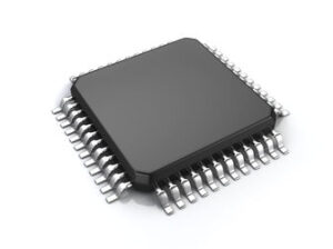
MCU 8-bit HCS08 S08 CISC 16KB Flash 3.3/5V 48-Pin QFP T/R, S9S08MP16E2MLFR, NXP

The S08MP16 is a cost-effective 8-bit MCU that delivers safe, accurate and inexpensive motor control for a wide range of industrial and automotive applications. An ideal entry-level solution for brushless DC (BLDC) motor applications, it features an 8-channel pulse width modulator (PWM)/flextimer module providing hardware dead-time insertion, analog comparators, programmable gain amplifier and a 12-bit analog-to-digital converter (ADC) with PWM hardware triggering. Also offered is an independently clocked COP and cyclic redundancy check (CRC) engine providing clock failure protection and memory content validation for safety-critical applications implementing IEC60730.

S08 Central Processor Unit (CPU)

  • Up to 50 MHz HCS08 CPU @ 2.7–5.5V across a temperature range of -40°C to +105°C
  • HCS08 instruction set with added BGND instruction

On-Chip Memory

  • Up to 16 KB flash read/program/erase over full operating voltage and temperature range
  • Up to 1 KB RAM
  • Security circuitry to prevent unauthorized access to RAM and flash contents

Power Saving Modes

  • Two low-power Stop modes and reduced power Wait mode
  • Peripheral clock gating can disable clocks to unused modules

Peripherals

  • Analog-to-digital converter (ADC)
    • 13 channels
    • 12-bit resolution
    • 2.5 µs conversion time
    • Automatic compare function
    • 1.7 mV/°C temperature sensor
    • Internal bandgap reference channel
    • Operation in stop 3 mode
  • 1 x 2-ch. FlexTimer + 1 x 6-ch
    • Supports up to 51.34 MHz operation
    • Selectable input capture
    • Output compare
    • Edgeor center-aligned PWM
    • Dead time insertion
    • Fault inputs
  • MTIM: simple 8-bit timer with four software-selectable clock sources and a programmable interrupt
  • 3 x high-speed analog comparators (HSACMP)
    • +ve and -ve inputs
    • Separately selectable interrupt on rising and falling comparator output
    • Filtering
    • Windowing
    • HSCMP1 and HSCMP2 outputs can be optionally routed to FTM1 modul
    • Runs in stop3
  • Programmable gain amplifier (PGA)
    • Differential programmable gain amplifier with programmable gain (x1, x2, x4, x8, x16 or x32)
  • 2 x programmable delay blocks (PDB)
    • PDB1 synchronizes PWM with samples of ADC
    • PDB2 synchronizes PWM with comparing window of analog comparators
  • Independently clocked COP and cyclic redundancy check generator

Development Support

  • Single-wire background debug interface
  • Breakpoint capability
  • ICE debug module
    • Three comparators and nine trigger modes
    • Eight deep FIFO for storing change-of-flow addresses and event-only data
    • Supports both tag and force breakpoints
Характеристики

Analog_comparators

3

Operating_supply_voltage

3.3, 5 V

Max_operating_supply_voltage

5.5 V

Watchdog

1

Supplier_package

QFP

Specifications

https://4donline.ihs.com/images/VipMasterIC/IC/FSCL/FSCLS05342/FSCLS05342-1.pdf?hkey=52A5661711E402568146F3353EA87419

Screening_level

Automotive

Schedule_b

8542310000

Ram_size

1 KB

Program_memory_type

Flash

Program_memory_size

16 KB

Product_dimensions

7 x 7 x 1.4

Pin_count

48

Operating_temperature

-40 to 125 °C

On_chip_adc

13-chx12-bit

Бренд

Number_of_timers

16

Number_of_programmable_i_os

40

Msl_level

3

Mounting

Surface Mount

Maximum_speed

40 MHz

Max_processing_temp

260

Тип интерфейса

I2C/SCI/SMBus/SPI

Instruction_set_architecture

CISC

Htsn

8542310001

Eccn

EAR99

Device_core

S08

Data_bus_width

8 Bit

Country_of_origin

China

Min_operating_supply_voltage

2.7 V

Артикул: S9S08MP16E2MLFR

Описание

The S08MP16 is a cost-effective 8-bit MCU that delivers safe, accurate and inexpensive motor control for a wide range of industrial and automotive applications. An ideal entry-level solution for brushless DC (BLDC) motor applications, it features an 8-channel pulse width modulator (PWM)/flextimer module providing hardware dead-time insertion, analog comparators, programmable gain amplifier and a 12-bit analog-to-digital converter (ADC) with PWM hardware triggering. Also offered is an independently clocked COP and cyclic redundancy check (CRC) engine providing clock failure protection and memory content validation for safety-critical applications implementing IEC60730.

S08 Central Processor Unit (CPU)

  • Up to 50 MHz HCS08 CPU @ 2.7–5.5V across a temperature range of -40°C to +105°C
  • HCS08 instruction set with added BGND instruction

On-Chip Memory

  • Up to 16 KB flash read/program/erase over full operating voltage and temperature range
  • Up to 1 KB RAM
  • Security circuitry to prevent unauthorized access to RAM and flash contents

Power Saving Modes

  • Two low-power Stop modes and reduced power Wait mode
  • Peripheral clock gating can disable clocks to unused modules

Peripherals

  • Analog-to-digital converter (ADC)
    • 13 channels
    • 12-bit resolution
    • 2.5 µs conversion time
    • Automatic compare function
    • 1.7 mV/°C temperature sensor
    • Internal bandgap reference channel
    • Operation in stop 3 mode
  • 1 x 2-ch. FlexTimer + 1 x 6-ch
    • Supports up to 51.34 MHz operation
    • Selectable input capture
    • Output compare
    • Edgeor center-aligned PWM
    • Dead time insertion
    • Fault inputs
  • MTIM: simple 8-bit timer with four software-selectable clock sources and a programmable interrupt
  • 3 x high-speed analog comparators (HSACMP)
    • +ve and -ve inputs
    • Separately selectable interrupt on rising and falling comparator output
    • Filtering
    • Windowing
    • HSCMP1 and HSCMP2 outputs can be optionally routed to FTM1 modul
    • Runs in stop3
  • Programmable gain amplifier (PGA)
    • Differential programmable gain amplifier with programmable gain (x1, x2, x4, x8, x16 or x32)
  • 2 x programmable delay blocks (PDB)
    • PDB1 synchronizes PWM with samples of ADC
    • PDB2 synchronizes PWM with comparing window of analog comparators
  • Independently clocked COP and cyclic redundancy check generator

Development Support

  • Single-wire background debug interface
  • Breakpoint capability
  • ICE debug module
    • Three comparators and nine trigger modes
    • Eight deep FIFO for storing change-of-flow addresses and event-only data
    • Supports both tag and force breakpoints
Детали

Analog_comparators

3

Operating_supply_voltage

3.3, 5 V

Max_operating_supply_voltage

5.5 V

Watchdog

1

Supplier_package

QFP

Specifications

https://4donline.ihs.com/images/VipMasterIC/IC/FSCL/FSCLS05342/FSCLS05342-1.pdf?hkey=52A5661711E402568146F3353EA87419

Screening_level

Automotive

Schedule_b

8542310000

Ram_size

1 KB

Program_memory_type

Flash

Program_memory_size

16 KB

Product_dimensions

7 x 7 x 1.4

Pin_count

48

Operating_temperature

-40 to 125 °C

On_chip_adc

13-chx12-bit

Бренд

Number_of_timers

16

Number_of_programmable_i_os

40

Msl_level

3

Mounting

Surface Mount

Maximum_speed

40 MHz

Max_processing_temp

260

Тип интерфейса

I2C/SCI/SMBus/SPI

Instruction_set_architecture

CISC

Htsn

8542310001

Eccn

EAR99

Device_core

S08

Data_bus_width

8 Bit

Country_of_origin

China

Min_operating_supply_voltage

2.7 V