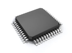
MCU 8-bit HCS08 CISC 96KB Flash 3.3V/5V 48-Pin LQFP Tray, S9S08DZ96F2MLF, NXP

The S08D family offers designers scalability and flexibility of migration with pin, peripheral and tool compatibility between S08D family devices. This highly integrated next generation family of MCUs is packed with features designed to provide increased performance, as well as save power, development time, board space and cost.

S08 CPU

  • 40 MHz core speed, 20 MHz bus speed on S08 CPU
  • HC08 instruction set with added BGND instruction

On-Chip Memory

  • Up to 128 KB flash read/program/erase over full operating voltage and temperature
  • Up to 2 KB EEPROM in-circuit programmable memory; 8-byte single-page or 4-byte dualpage erase sector; program and erase while executing flash; erase abort
  • Up to 8 KB RAM (16:1 flash/RAM, ratio better than competition)

Power Saving Modes

  • Two very low-power stop modes
  • Very low-power, real-time interrupt for use in run, wait and stop modes

Clock Source Options

  • Oscillator (XOSC)—Loop-control Pierce oscillator; crystal or ceramic resonator range of 31.25 kHz–38.4 kHz or 1 MHz–16 MHz
  • Multi-purpose clock generator (MCG)–PLL and FLL modes; internal reference clock with trim adjustment; external reference with oscillator/resonator options

System Protection

  • Watchdog computer operating properly (COP) reset with option to run from dedicated 1 kHz internal clock source or bus clock
  • Low-voltage detection with reset or interrupt; selectable trip points
  • Illegal opcode detection with reset
  • Illegal address detection with reset
  • Flash block protect
  • EEPROM block protect

Peripherals

  • ACMPx—Analog comparators with selectable interrupt on rising, falling or either edge of comparator output; compare option to fixed internal bandgap reference voltage
  • MSCAN—CAN protocol—Version 2.0 A, B; standard and extended data frames; support for remote frames; five receive buffers with FIFO storage scheme; flexible identifier acceptance filters programmable as: 2 x 32-bit, 4 x 16-bit, or 8 x 8-bit
  • SCIx—SCI(s) with LIN 2.0 Protocol and SAE J2602 compliance; master extended break generation; slave extended break detection; LIN slave supplement on SCI1; automatic baud rate correction; message time-out detection
  • SPI—Full-duplex or single-wire bi-directional; double-buffered transmit and receive; master or slave mode; MSB-first or LSB-first shifting
  • I2C—Up to 100 kbps with maximum bus loading; multi-master operation; programmable slave address; interrupt-driven, byte-by-byte data transfer; broadcast mode enabled
  • TPMx—One 6-channel (TMP1) and one 2-channel (TPM2); selectable input capture, output compare or buffered edge-aligned PWM on each channel
  • RTC (Real-time counter)—8-bit modulus counter with binary or decimal-based prescaler; external clock source for precise time base, time-of-day calendar or task scheduling functions; free running, on-chip, low-power oscilator (1 kHz) for cyclic wake-up without external components

Development Support

  • Single-wire background debug (BDM) interface
  • On-chip, in-circuit emulation (ICE) with real-time bus capture

Input/Output

  • 87 general-purpose I/O pins and one input-only pin
  • 32 interrupt pins with selectable polarity on each pin
  • Hysteresis and configurable pull-up device on all input pins
  • Configurable slew rate and device strength on all output pins

Package Options

  • 100 LQFP 14 x 14 mm
  • 64-pin low-profile quad flat pack (LQFP)—10 x 10 mm
  • 48-pin LQFP—7 x 7 mm
  • 32-pin LQFP—7 x 7 mm

Miscellaneous

  • EMC performance
  • Wide operating voltage range: 2.7V–5.5V

Background Debugging System

  • On-chip BDM

Package

  • Pin-compatible with SH, QG family

Product Longevity Program
Характеристики

Analog_comparators

2

On_chip_adc

16-chx12-bit

Min_operating_supply_voltage

2.7 V

Max_operating_supply_voltage

5.5 V

Watchdog

1

Supplier_package

LQFP

Specifications

http://www.freescale.com/files/microcontrollers/doc/data_sheet/MC9S08DZ128.pdf

Schedule_b

8541290080

Ram_size

6 KB

Program_memory_type

Flash

Program_memory_size

96 Kb

Product_dimensions

7 x 7 x 1.45 mm

Pin_count

48

Operating_temperature

-40 to 125 °C

Operating_supply_voltage

3.3, 5 V

Number_of_programmable_i_os

87

Бренд

Msl_level

3

Mounting

Surface Mount

Maximum_speed

40 MHz

Max_processing_temp

260

Lead_finish

Matte Tin

Тип интерфейса

CAN/I2C/SCI/SPI

Instruction_set_architecture

CISC

Htsn

8541290075

Eccn

3A991.A.2

Data_memory_size

2048 byte

Data_bus_width

8 Bit

Country_of_origin

China

Max_expanded_memory_size

128 KB

Артикул: S9S08DZ96F2MLF

Описание

The S08D family offers designers scalability and flexibility of migration with pin, peripheral and tool compatibility between S08D family devices. This highly integrated next generation family of MCUs is packed with features designed to provide increased performance, as well as save power, development time, board space and cost.

S08 CPU

  • 40 MHz core speed, 20 MHz bus speed on S08 CPU
  • HC08 instruction set with added BGND instruction

On-Chip Memory

  • Up to 128 KB flash read/program/erase over full operating voltage and temperature
  • Up to 2 KB EEPROM in-circuit programmable memory; 8-byte single-page or 4-byte dualpage erase sector; program and erase while executing flash; erase abort
  • Up to 8 KB RAM (16:1 flash/RAM, ratio better than competition)

Power Saving Modes

  • Two very low-power stop modes
  • Very low-power, real-time interrupt for use in run, wait and stop modes

Clock Source Options

  • Oscillator (XOSC)—Loop-control Pierce oscillator; crystal or ceramic resonator range of 31.25 kHz–38.4 kHz or 1 MHz–16 MHz
  • Multi-purpose clock generator (MCG)–PLL and FLL modes; internal reference clock with trim adjustment; external reference with oscillator/resonator options

System Protection

  • Watchdog computer operating properly (COP) reset with option to run from dedicated 1 kHz internal clock source or bus clock
  • Low-voltage detection with reset or interrupt; selectable trip points
  • Illegal opcode detection with reset
  • Illegal address detection with reset
  • Flash block protect
  • EEPROM block protect

Peripherals

  • ACMPx—Analog comparators with selectable interrupt on rising, falling or either edge of comparator output; compare option to fixed internal bandgap reference voltage
  • MSCAN—CAN protocol—Version 2.0 A, B; standard and extended data frames; support for remote frames; five receive buffers with FIFO storage scheme; flexible identifier acceptance filters programmable as: 2 x 32-bit, 4 x 16-bit, or 8 x 8-bit
  • SCIx—SCI(s) with LIN 2.0 Protocol and SAE J2602 compliance; master extended break generation; slave extended break detection; LIN slave supplement on SCI1; automatic baud rate correction; message time-out detection
  • SPI—Full-duplex or single-wire bi-directional; double-buffered transmit and receive; master or slave mode; MSB-first or LSB-first shifting
  • I2C—Up to 100 kbps with maximum bus loading; multi-master operation; programmable slave address; interrupt-driven, byte-by-byte data transfer; broadcast mode enabled
  • TPMx—One 6-channel (TMP1) and one 2-channel (TPM2); selectable input capture, output compare or buffered edge-aligned PWM on each channel
  • RTC (Real-time counter)—8-bit modulus counter with binary or decimal-based prescaler; external clock source for precise time base, time-of-day calendar or task scheduling functions; free running, on-chip, low-power oscilator (1 kHz) for cyclic wake-up without external components

Development Support

  • Single-wire background debug (BDM) interface
  • On-chip, in-circuit emulation (ICE) with real-time bus capture

Input/Output

  • 87 general-purpose I/O pins and one input-only pin
  • 32 interrupt pins with selectable polarity on each pin
  • Hysteresis and configurable pull-up device on all input pins
  • Configurable slew rate and device strength on all output pins

Package Options

  • 100 LQFP 14 x 14 mm
  • 64-pin low-profile quad flat pack (LQFP)—10 x 10 mm
  • 48-pin LQFP—7 x 7 mm
  • 32-pin LQFP—7 x 7 mm

Miscellaneous

  • EMC performance
  • Wide operating voltage range: 2.7V–5.5V

Background Debugging System

  • On-chip BDM

Package

  • Pin-compatible with SH, QG family

Product Longevity Program

Детали

Analog_comparators

2

On_chip_adc

16-chx12-bit

Min_operating_supply_voltage

2.7 V

Max_operating_supply_voltage

5.5 V

Watchdog

1

Supplier_package

LQFP

Specifications

http://www.freescale.com/files/microcontrollers/doc/data_sheet/MC9S08DZ128.pdf

Schedule_b

8541290080

Ram_size

6 KB

Program_memory_type

Flash

Program_memory_size

96 Kb

Product_dimensions

7 x 7 x 1.45 mm

Pin_count

48

Operating_temperature

-40 to 125 °C

Operating_supply_voltage

3.3, 5 V

Number_of_programmable_i_os

87

Бренд

Msl_level

3

Mounting

Surface Mount

Maximum_speed

40 MHz

Max_processing_temp

260

Lead_finish

Matte Tin

Тип интерфейса

CAN/I2C/SCI/SPI

Instruction_set_architecture

CISC

Htsn

8541290075

Eccn

3A991.A.2

Data_memory_size

2048 byte

Data_bus_width

8 Bit

Country_of_origin

China

Max_expanded_memory_size

128 KB