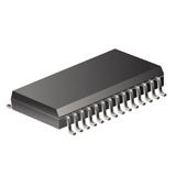
MCU 8-bit HC08 CISC 8KB Flash 3.3V/5V 28-Pin SOIC W Rail, MC908QC8CDZE, NXP

The MC68HC908QC16, MC68HC908QC8, and MC68HC908QC4 are members of the low-cost, high-performance M68HC08 Family of 8-bit microcontroller units (MCUs). All MCUs in the family use the enhanced M68HC08 central processor unit (CPU08) and are available with a variety of modules, memory sizes and types, and package types.

  • High-performance M68HC08 CPU core
  • Fully upward-compatible object code with M68HC05 Family
  • 5.0-V and 3.3-V operating voltages (VDD)
  • 8-MHz internal bus operation at 5 V, 4-MHz at 3.3 V
  • Trimmable internal oscillator
    • Software selectable 1 MHz, 2 MHz, 3.2 MHz, or 6.4 MHz internal bus operation
    • 8-bit trim capability
    • 25% untrimmed
    • Trimmable to approximately 0.4%(1)
  • Software selectable crystal oscillator range, 32
    • 100 kHz, 1
    • 8 MHz, and 8
    • 32 MHz
  • Software configurable input clock from either internal or external source
  • Auto wakeup from STOP capability using dedicated internal 32-kHz RC or bus clock source
  • FLASH security(2)
  • On-chip in-application programmable FLASH memory (with internal program/erase voltage generation)
  • Enhanced serial communications interface (ESCI) module
  • Serial peripheral interface (SPI) module
  • 4-channel, 16-bit timer interface (TIM1) module
  • 2-channel, 16-bit timer interface (TIM2) module
  • 10-channel, 10-bit analog-to-digital converter (ADC) with internal bandgap reference channel (ADC10)
  • Up to 24 bidirectional input/output (I/O) lines and two input only:
    • Six shared with keyboard interrupt function
    • Ten shared with ADC
    • Four shared with TIM1
    • Two shared with TIM2
    • Two shared with ESCI
    • Four shared with SPI
    • One input only shared with external interrupt (IRQ)
    • High current sink/source capability on all port pins
    • Selectable pullups on all ports, selectable on an individual bit basis
    • Three-state ability on all port pins
  • 6-bit keyboard interrupt with wakeup feature (KBI)
    • Programmable for rising/falling edge or high/low level detection
  • Low-voltage inhibit (LVI) module features:
    • Software selectable trip point in CONFIG register
  • System protection features:
    • Computer operating properly (COP) watchdog
    • Low-voltage detection with reset
    • Illegal opcode detection with reset
    • Illegal address detection with reset
  • External asynchronous interrupt pin with internal pullup (IRQ) shared with general-purpose input pin
  • Master asynchronous reset pin with internal pullup (RST) shared with general-purpose input/output (I/O) pin
  • Memory mapped I/O registers
  • Power saving stop and wait modes
  • MC68HC908QC16, MC68HC908QC8, and MC68HC908QC4 are available in these packages:
    • 28-pin small outline integrated circuit package (SOIC)
    • 28-pin thin shrink small outline package (TSSOP)
    • 20-pin SOIC
    • 20-pin TSSOP
    • 16-pin SOIC
    • 16-pin TSSOP

Характеристики

Бренд

Operating_supply_voltage

3.3, 5 V

Min_operating_supply_voltage

3 V

Max_operating_supply_voltage

5.5 V

Watchdog

1

Supplier_package

SOIC W

Specifications

https://4donline.ihs.com/images/VipMasterIC/IC/PHGL/PHGL-S-A0002318245/PHGL-S-A0002318245-1.pdf?hkey=52A5661711E402568146F3353EA87419

Schedule_b

8542310000

Ram_size

384 byte

Program_memory_type

Flash

Program_memory_size

8 KB

Product_dimensions

18.05 x 7.6 x 2.36 mm

Pin_count

28

Operating_temperature

-40 to 85 °C

On_chip_adc

10-chx10-bit

Country_of_origin

United States

Number_of_timers

6

Number_of_programmable_i_os

26

Msl_level

3

Mounting

Surface Mount

Maximum_speed

8 MHz

Max_processing_temp

260

Lead_finish

Matte Tin

Тип интерфейса

SCI/SPI

Instruction_set_architecture

CISC

Htsn

8542310001

Eccn

3A991.A.2

Data_bus_width

8 Bit

Max_expanded_memory_size

64 KB

Артикул: MC908QC8CDZE

Описание

The MC68HC908QC16, MC68HC908QC8, and MC68HC908QC4 are members of the low-cost, high-performance M68HC08 Family of 8-bit microcontroller units (MCUs). All MCUs in the family use the enhanced M68HC08 central processor unit (CPU08) and are available with a variety of modules, memory sizes and types, and package types.

  • High-performance M68HC08 CPU core
  • Fully upward-compatible object code with M68HC05 Family
  • 5.0-V and 3.3-V operating voltages (VDD)
  • 8-MHz internal bus operation at 5 V, 4-MHz at 3.3 V
  • Trimmable internal oscillator
    • Software selectable 1 MHz, 2 MHz, 3.2 MHz, or 6.4 MHz internal bus operation
    • 8-bit trim capability
    • 25% untrimmed
    • Trimmable to approximately 0.4%(1)
  • Software selectable crystal oscillator range, 32
    • 100 kHz, 1
    • 8 MHz, and 8
    • 32 MHz
  • Software configurable input clock from either internal or external source
  • Auto wakeup from STOP capability using dedicated internal 32-kHz RC or bus clock source
  • FLASH security(2)
  • On-chip in-application programmable FLASH memory (with internal program/erase voltage generation)
  • Enhanced serial communications interface (ESCI) module
  • Serial peripheral interface (SPI) module
  • 4-channel, 16-bit timer interface (TIM1) module
  • 2-channel, 16-bit timer interface (TIM2) module
  • 10-channel, 10-bit analog-to-digital converter (ADC) with internal bandgap reference channel (ADC10)
  • Up to 24 bidirectional input/output (I/O) lines and two input only:
    • Six shared with keyboard interrupt function
    • Ten shared with ADC
    • Four shared with TIM1
    • Two shared with TIM2
    • Two shared with ESCI
    • Four shared with SPI
    • One input only shared with external interrupt (IRQ)
    • High current sink/source capability on all port pins
    • Selectable pullups on all ports, selectable on an individual bit basis
    • Three-state ability on all port pins
  • 6-bit keyboard interrupt with wakeup feature (KBI)
    • Programmable for rising/falling edge or high/low level detection
  • Low-voltage inhibit (LVI) module features:
    • Software selectable trip point in CONFIG register
  • System protection features:
    • Computer operating properly (COP) watchdog
    • Low-voltage detection with reset
    • Illegal opcode detection with reset
    • Illegal address detection with reset
  • External asynchronous interrupt pin with internal pullup (IRQ) shared with general-purpose input pin
  • Master asynchronous reset pin with internal pullup (RST) shared with general-purpose input/output (I/O) pin
  • Memory mapped I/O registers
  • Power saving stop and wait modes
  • MC68HC908QC16, MC68HC908QC8, and MC68HC908QC4 are available in these packages:
    • 28-pin small outline integrated circuit package (SOIC)
    • 28-pin thin shrink small outline package (TSSOP)
    • 20-pin SOIC
    • 20-pin TSSOP
    • 16-pin SOIC
    • 16-pin TSSOP

Детали

Бренд

Operating_supply_voltage

3.3, 5 V

Min_operating_supply_voltage

3 V

Max_operating_supply_voltage

5.5 V

Watchdog

1

Supplier_package

SOIC W

Specifications

https://4donline.ihs.com/images/VipMasterIC/IC/PHGL/PHGL-S-A0002318245/PHGL-S-A0002318245-1.pdf?hkey=52A5661711E402568146F3353EA87419

Schedule_b

8542310000

Ram_size

384 byte

Program_memory_type

Flash

Program_memory_size

8 KB

Product_dimensions

18.05 x 7.6 x 2.36 mm

Pin_count

28

Operating_temperature

-40 to 85 °C

On_chip_adc

10-chx10-bit

Country_of_origin

United States

Number_of_timers

6

Number_of_programmable_i_os

26

Msl_level

3

Mounting

Surface Mount

Maximum_speed

8 MHz

Max_processing_temp

260

Lead_finish

Matte Tin

Тип интерфейса

SCI/SPI

Instruction_set_architecture

CISC

Htsn

8542310001

Eccn

3A991.A.2

Data_bus_width

8 Bit

Max_expanded_memory_size

64 KB