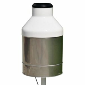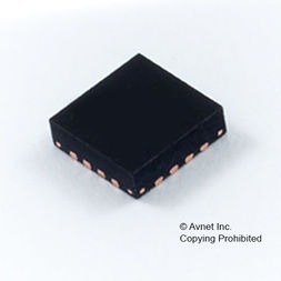
Описание
The enCoRe V LV family of devices are designed to replace multiple traditional low voltage microcontroller system components with one, low cost single chip programmable component. Communication peripherals (I2C/SPI), a fast CPU, Flash program memory, SRAM data memory, and configurable I/O are included in a range of convenient pinoutsThe architecture for this device family, as illustrated in enCoRe V LV Block Diagram, is comprised of two main areas: the CPU core and the system resources. Depending on the enCoRe V LV package, up to 36 general purpose IO (GPIO) are also included. Enhancements over the Cypress’s legacy low voltage microcontrollers include faster CPU at lower voltage operation, lower current consumption, twice the RAM and Flash, hot-swapable I/Os, I2C hardware address recognition, new very low current sleep mode, and new package options.The enCoRe V LV Core is a powerful engine that supports a rich instruction set. It encompasses SRAM for data storage, an interrupt controller, sleep and watchdog timers, and IMO (internal main oscillator) and ILO (internal low speed oscillator). The CPU core, called the M8C, is a powerful processor with speeds up to 24 MHz. The M8C is a four-MIPS, 8-bit Harvard architecture microprocessor.System Resources provide additional capability, such as a configurable I2C slave and SPI master-slave communication interface and various system resets supported by the M8C.The ADC on enCoRe V LV device is an independent block with a state machine interface to control accesses to the block. The ADC is housed together with the temperature sensor core and can be connected to this or the Analog Mux Bus. As a default operation, the ADC is connected to the temperature sensor diodes to give digital values of the temperature.The ADC User Module contains an integrator block and one comparator with positive and negative input set by the MUXes. The input to the integrator stage comes from the Analog Global Input Mux or the temperature sensor with an input voltage range of 0V to 1.3 V, where 1.3V is 72% of full scale.In the ADC only configuration (the ADC MUX selects the Analog Mux Bus, not the default temperature sensor connection), an external voltage can be connected to the input of the modulator for voltage conversion. The ADC is run for a number of cycles set by the timer, depending upon the resolution of the ADC desired by the user. A counter counts the number of trips by the comparator, which is proportional to the input voltage. The Temp Sensor block clock speed is 36 MHz and is divided down to 1 to 12 MHz for ADC operation.
- Powerful Harvard Architecture Processor
- M8C processor speeds running up to 24 MHz
- Low power at high processing speeds
- Interrupt controller
- 1.71V to 3.6V operating voltage
- Commercial temperature range: 0°C to +70°C
- Flexible On-Chip Memory
- Up to 32K Flash program storage
- 50,000 Erase and write cycles
- Flexible protection modes
- Up to 2048 bytes SRAM data storage
- In-System Serial Programming (ISSP)
- Complete Development Tools
- Free development tool (PSoC Designer™)
- Full featured, in-circuit emulator and programmer
- Full speed emulation
- Complex breakpoint structure
- 128K trace memory
- Precision, Programmable Clocking
- Crystal-less oscillator with support for an external crystal or resonator
- Internal ±5.0% 6, 12, or 24 MHz main oscillator
- Internal low speed oscillator at 32 kHz for watchdog and sleep.The frequency range is 19 to 50 kHz with a 32 kHz typical value Programmable Pin Configurations
- Up to 36 GPIO (Depending on Package)
- 25 mA sink current on all GPIO
- Pull Up, High Z, Open Drain, CMOS drive modes on all GPIO
- CMOS Drive Mode (5 mA Source Current) on Ports 0 and 1:
- 20 mA (at 3.0V) Total Source Current
- Low dropout voltage regulator for Port 1 pins:
- Programmable to output 3.0, 2.5, or 1.8V
- Selectable, regulated digital I/O on Port 1
- Configurable input threshold for Port 1
- Hot-swappable Capability on Port 1
- Additional System Resources
- Configurable communication speeds
- I2C Slave
- Selectable to 50 kHz, 100 kHz, or 400 kHz
- Implementation requires no clock stretching
- Implementation during sleep modes with less than 100 mA
- Hardware address detection
- SPI master and SPI slave
- Configurable between 46.9 kHz and 12 MHz
- Three 16-bit timers
- 10-bit ADC used to monitor battery voltage or other signals with external components
- Watchdog and sleep timers
- Integrated supervisory circuit