Описание
The enCoRe II LV family brings the features and benefits of the enCoRe II to non-USB applications. The enCoRe II family has an integrated oscillator that eliminates the external crystal or resonator, reducing overall cost. Other external components, such as wake-up circuitry, are also integrated into this chip.The enCoRe II LV is a low-voltage, low-cost 8-bit Flashprogrammable microcontrollerThe enCoRe II LV features up to 36 general-purpose I/O (GPIO) pins. The I/O pins are grouped into five ports (Port 0 to 4). The pins on Port 0 and Port 1 may each be configured individually while the pins on Ports 2, 3, and 4 may only be configured as a group. Each GPIO port supports highimpedance inputs, configurable pull up, open drain output, CMOS/TTL inputs, and CMOS output with up to five pins that support programmable drive strength of up to 50 mA sink current. Additionally, each I/O pin can be used to generate a GPIO interrupt to the microcontroller. Each GPIO port has its own GPIO interrupt vector with the exception of GPIO Port 0. GPIO Port 0 has in addition to the port interrupt vector, three dedicated pins that have independent interrupt vectors (P0.2–P0.4)The enCoRe II LV features an internal oscillator. Optionally, an external 1 MHz to 24 MHz crystal can be used to provide a higher precision reference. The enCoRe II LV also supports external clockThe enCoRe II LV has 8 Kbytes of Flash for user’s code and 256 bytes of RAM for stack space and user variablesIn addition, enCoRe II LV includes a Watchdog timer, a vectored interrupt controller, a 16-bit Free-Running Timer with Capture registers and a 12-bit Programmable Interval Timer. The Power-on reset circuit detects when power is applied to the device, resets the logic to a known state, and begins executing instructions at Flash address 0x0000. When power falls below a programmable trip voltage it generates a reset or may be configured to generate an interrupt. There is a Lowvoltage detect circuit that detects when VCC drops below a programmable trip voltage and it may be configurable to generate a LVD interrupt to inform the processor about the low-voltage event. POR and LVD share the same interrupt; there is no separate interrupt for each. The Watchdog timer can be used to ensure the firmware never gets stalled in an infinite loopThe microcontroller supports 17 maskable interrupts in the vectored interrupt controller. All interrupts can be masked. Interrupt sources include LVR/POR, a programmable interval timer, a nominal 1.024-ms programmable output from the Free Running Timer, two capture timers, five GPIO Ports, three GPIO pins, two SPI, a 16-bit free-running timer wrap and an internal wakeup timer interrupt. The wakeup timer causes periodic interrupts when enabled. The capture timers interrupt whenever a new timer value is saved due to a selected GPIO edge event. A total of eight GPIO interrupts support both TTL or CMOS thresholds. For additional flexibility, on the edgesensitive GPIO pins, the interrupt polarity is programmable to be either rising or falling. The free-running timer generates an interrupt at 1024-µs rate. It can also generate an interrupt when the free-running counter overflow occurs—every 16.384 ms. The timer can be used to measure the duration of an event under firmware control by reading the timer at the start and at the end of an event, then calculating the difference between the two values. The two 8- bit capture timer registers save a programmable 8-bit range of the free-running timer when a GPIO edge occurs on the two capture pins (P0.5, P0.6). The two 8-bit capture registers can be ganged into a single 16-bit capture register.The enCoRe II LV supports in-system programming by using the P1.0 and P1.1 pins as the serial programming mode interface.
- enCoRe™ II Low Voltage (enCoRe II LV)
- “enhanced Component Reduction”
- Internal crystalless oscillator with support for optional external clock or external crystal or resonator.
- Configurable IO for real-world interface without external components
- Enhanced 8-bit microcontroller
- Harvard architecture
- M8C CPU speed can be up to 12 MHz or sourced by an external crystal, resonator, or clock signal
- Internal memory
- 256 bytes of RAM
- 8 Kbytes of Flash including EEROM emulation
- Low power consumption
- Typically 2.25 mA at 3 MHz
- 5 µA sleep
- In-system reprogrammability
- Allows easy firmware update
- General-purpose I/O ports
- Up to 36 General Purpose I/O (GPIO) pins
- High current drive on GPIO pins. Configurable 8- or 50-mA/pin current sink on designated pins
- Each GPIO port supports high-impedance inputs, configurable pull-up, open drain output, CMOS/TTL inputs, and CMOS output
- Maskable interrupts on all I/O pins
- SPI serial communication
- Master or slave operation
- Configurable up to 2-Mbit/second transfers.
- Supports half duplex single data line mode for optical sensors
- 2-channel 8-bit or 1-channel 16-bit capture timer registers. Capture timer registers store both rising and falling edge times
- Two registers each for two input pins
- Separate registers for rising and falling edge capture
- Simplifies interface to RF inputs for wireless applications
- Internal low-power wake-up timer during suspend mode
- Periodic wake-up with no external components
- Programmable Interval Timer interrupts
- Reduced RF emissions at 27 MHz and 96 MHz
- Watchdog timer (WDT)
- Low voltage detection with user-selectable threshold voltages Improved output drivers to reduce EMI
- Operating voltage from 2.7V to 3.6VDC
- Operating temperature from 0-70°C
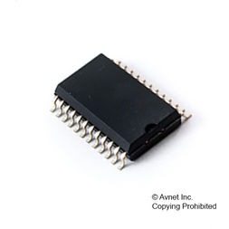
- Available in 24/40-pin PDIP, 24-pin SOIC, 24-pin QSOP/SSOP, 28-pin SSOP and 48-pin SSOP.
- Advanced development tools based on Cypress PSoC® tools
- Industry-standard programmer support