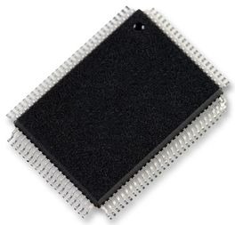
MCU 8-Bit DS52xx 8051 CISC ROMLess 100-Pin MQFP, DS5240F-1N5+, Maxim Integrated

The DS5240F-1N5+ is a high-speed 8051 compatible security processor with built-in system features designed to meet the stringent FIPS-140 and Common Criteria validations required by banking regulations worldwide. Based on Dallas Semiconductor’s battery-backed technology and fast-erase SRAM design, the DS5240F-1N5+ supports rapid “zeroization” of secure information as a tamper response. Security-related features included on-chip are a fine-line top-level metal grid to protect underlying circuitry from tampering, a Modulo Arithmetic Accelerator (MAA) using words up to 4096-bits in length for calculations including Public Key Infrastructure (PKI), a random number generator for key creation, multiple on-chip environmental sensors to detect out-of-range conditions and generate a tamper response, and a user-available DES engine for arbitrary data encryption. The user DES engine supports both single and triple-DES (3DES) cryptographic operations. Other on-chip features include a true-time clock with alarm interrupt/wake-up capability, a CRC-16/32 generator, a phase-locked loop (PLL) to simplify crystal selection and to isolate internal chip clocks from external system clock, extended memory addressing of up to 4MB program and 4MB data and a 1kB stack (part of 5kB total SRAM) for high-level language support, circuitry to control battery backing of certain internal circuits and external SRAM for storage of program and/or data, and sleep, idle and power management modes for low power applications. The DS5240F-1N5+’s comprehensive security measures create a trusted computing environment for the most sensitive applications. These measures include an array of features specifically designed to resist known threats including observation, analysis, and physical attack. They are designed such that a massive effort would be required to obtain information about the contents of the chip (e.g., stored encryption keys) and/or external memory. Furthermore, the “soft” nature of the DS5240F-1N5+ (SRAM storage) allows frequent modification of secure information, either program or data.

  • Security Features
    • Designed to Meet the Physical Security
    • Requirements of FIPS140 and Common Criteria Certifications
    • Fine-Line, Top-Level Metal Pattern Detects
    • intrusion of the Chip’s Cryptographic Boundary
    • Additional On-Chip Sensors Detect Out-of-Range
    • Environmental Conditions That Generate a Tamper Response
    • Equipment Enclosure Can Be Monitored by
    • Tamper Response Inputs for Added Protection
    • Fast Write SRAM Technology Causes Rapid
    • “Zeroization” of Secure Information as a Tamper Response
    • Eavesdropping on the External Memory Bus
    • Prevented by Single or Triple-DES
    • Encryption of the Programs
    • Internal Chip Clock Isolated from External System
    • Clock by Phase-Locked Loop
    • Asynchronous Internal Ring Oscillator Provides
    • Clock for Arithmetic Operations
    • Resources Inside Cryptographic Boundary Include:
    • Modulo Arithmetic Accelerator (MAA) for Up to 4096-Bit (e.g., PKI) DES and 112-Bit Key Triple-DES Engines Available for Secret Key Cryptography
    • Random Number Generator
    • Memory Management Unit and 1kB Cache
    • Firmware Bootstrap Loader Resides in a16kB Factory-Programmed ROM
  • 8051-Compatible with Expanded Addressing
    • Linear Address Space Directly Accesses Up to
    • 8MB of External Memory
    • Dedicated Memory and Parallel I/O Bus Saves Port Pins
    • Four 8-Bit Ports, One 6-Bit Port
  • Advanced Features
    • CRC-16/32 Generator Provides Strong Error Detection of Memory Contents
    • True-Time Clock with Alarm Interrupt and Wakeup 5kB Internal SRAM with 1kB That Can Be
    • Allocated to a Stack for High-Level Language SupportProgrammable Length MOVX Instructions Allow aCombination of Fast and Slow Devices
    • On-Chip Power Detection/Selection Circuits Provide Power-Up/Down Processor Reset and Early-Warning Power-Fail Interrupt Watchdog Timer
  • Proven 4-Clock/Machine Cycle Architecture
    • Single-Cycle Instruction Executes in 160ns
    • Runs Up to 25MHz Clock Rates
    • Dual Data Pointers Can Increment or Decrement Independently
    • Automatic Data Pointer Selection Available
  • -40°C to +85°C Temperature
  • 100-Plastic MQFP Package

Характеристики

Бренд

Number_of_programmable_i_os

38

Supplier_package

MQFP

Specifications

http://datasheets.maximintegrated.com/en/ds/DS5240.pdf

Screening_level

Industrial

Schedule_b

8541290080

Ram_size

5 KB

Program_memory_type

ROMLess

Product_dimensions

14 x 20 x 2.87(Max)

Pin_count

100

Operating_temperature

-40 to 85 °C

Number_of_timers

3

Msl_level

4

Country_of_origin

United States

Mounting

Surface Mount

Maximum_speed

25 MHz

Maximum_expanded_memory_size

8 MB

Lead_finish

Matte Tin

Instruction_set_architecture

CISC

Htsn

8541290075

Eccn

5A002.A.1

Device_core

8051

Watchdog

1

Max_expanded_memory_size

8 MB

Артикул: DS5240F-1N5+

Описание

The DS5240F-1N5+ is a high-speed 8051 compatible security processor with built-in system features designed to meet the stringent FIPS-140 and Common Criteria validations required by banking regulations worldwide. Based on Dallas Semiconductor’s battery-backed technology and fast-erase SRAM design, the DS5240F-1N5+ supports rapid “zeroization” of secure information as a tamper response. Security-related features included on-chip are a fine-line top-level metal grid to protect underlying circuitry from tampering, a Modulo Arithmetic Accelerator (MAA) using words up to 4096-bits in length for calculations including Public Key Infrastructure (PKI), a random number generator for key creation, multiple on-chip environmental sensors to detect out-of-range conditions and generate a tamper response, and a user-available DES engine for arbitrary data encryption. The user DES engine supports both single and triple-DES (3DES) cryptographic operations. Other on-chip features include a true-time clock with alarm interrupt/wake-up capability, a CRC-16/32 generator, a phase-locked loop (PLL) to simplify crystal selection and to isolate internal chip clocks from external system clock, extended memory addressing of up to 4MB program and 4MB data and a 1kB stack (part of 5kB total SRAM) for high-level language support, circuitry to control battery backing of certain internal circuits and external SRAM for storage of program and/or data, and sleep, idle and power management modes for low power applications. The DS5240F-1N5+’s comprehensive security measures create a trusted computing environment for the most sensitive applications. These measures include an array of features specifically designed to resist known threats including observation, analysis, and physical attack. They are designed such that a massive effort would be required to obtain information about the contents of the chip (e.g., stored encryption keys) and/or external memory. Furthermore, the “soft” nature of the DS5240F-1N5+ (SRAM storage) allows frequent modification of secure information, either program or data.

  • Security Features
    • Designed to Meet the Physical Security
    • Requirements of FIPS140 and Common Criteria Certifications
    • Fine-Line, Top-Level Metal Pattern Detects
    • intrusion of the Chip’s Cryptographic Boundary
    • Additional On-Chip Sensors Detect Out-of-Range
    • Environmental Conditions That Generate a Tamper Response
    • Equipment Enclosure Can Be Monitored by
    • Tamper Response Inputs for Added Protection
    • Fast Write SRAM Technology Causes Rapid
    • “Zeroization” of Secure Information as a Tamper Response
    • Eavesdropping on the External Memory Bus
    • Prevented by Single or Triple-DES
    • Encryption of the Programs
    • Internal Chip Clock Isolated from External System
    • Clock by Phase-Locked Loop
    • Asynchronous Internal Ring Oscillator Provides
    • Clock for Arithmetic Operations
    • Resources Inside Cryptographic Boundary Include:
    • Modulo Arithmetic Accelerator (MAA) for Up to 4096-Bit (e.g., PKI) DES and 112-Bit Key Triple-DES Engines Available for Secret Key Cryptography
    • Random Number Generator
    • Memory Management Unit and 1kB Cache
    • Firmware Bootstrap Loader Resides in a16kB Factory-Programmed ROM
  • 8051-Compatible with Expanded Addressing
    • Linear Address Space Directly Accesses Up to
    • 8MB of External Memory
    • Dedicated Memory and Parallel I/O Bus Saves Port Pins
    • Four 8-Bit Ports, One 6-Bit Port
  • Advanced Features
    • CRC-16/32 Generator Provides Strong Error Detection of Memory Contents
    • True-Time Clock with Alarm Interrupt and Wakeup 5kB Internal SRAM with 1kB That Can Be
    • Allocated to a Stack for High-Level Language SupportProgrammable Length MOVX Instructions Allow aCombination of Fast and Slow Devices
    • On-Chip Power Detection/Selection Circuits Provide Power-Up/Down Processor Reset and Early-Warning Power-Fail Interrupt Watchdog Timer
  • Proven 4-Clock/Machine Cycle Architecture
    • Single-Cycle Instruction Executes in 160ns
    • Runs Up to 25MHz Clock Rates
    • Dual Data Pointers Can Increment or Decrement Independently
    • Automatic Data Pointer Selection Available
  • -40°C to +85°C Temperature
  • 100-Plastic MQFP Package

Детали

Бренд

Number_of_programmable_i_os

38

Supplier_package

MQFP

Specifications

http://datasheets.maximintegrated.com/en/ds/DS5240.pdf

Screening_level

Industrial

Schedule_b

8541290080

Ram_size

5 KB

Program_memory_type

ROMLess

Product_dimensions

14 x 20 x 2.87(Max)

Pin_count

100

Operating_temperature

-40 to 85 °C

Number_of_timers

3

Msl_level

4

Country_of_origin

United States

Mounting

Surface Mount

Maximum_speed

25 MHz

Maximum_expanded_memory_size

8 MB

Lead_finish

Matte Tin

Instruction_set_architecture

CISC

Htsn

8541290075

Eccn

5A002.A.1

Device_core

8051

Watchdog

1

Max_expanded_memory_size

8 MB