MCU 8-Bit AX8052F143 8052 CISC 64KB Flash 1.8V to 3.6V 40-Pin QFN EP T/R, AX8052F143-3-TX40, ON Semiconductor

The AX8052F143 is a true single chip narrow-band, ultra-low power RF-microcontroller SoC for use in licensed and unlicensed bands ranging from 70 MHz to 1050 MHz The on-chip transceiver consists of a fully integrated RF front-end with modulator and demodulator. Base band data processing is implemented in an advanced and flexible communication controller that enables user friendly communication. The AX8052F143 contains a high speed microcontroller compatible to the industry standard 8052 instruction set. It contains 64 Kbytes of FLASH and 8.25 Kbytes of internal SRAM. The AX8052F143 features 3 16-bit general purpose timers with capability, 2 output compare units for generating PWM signals, 2 input compare units to record timings of external signals, 2 16-bit wakeup timers, a watchdog timer, 2 UARTs, a Master/Slave SPI controller, a 10-bit 500 kSample/s A/D converter, 2 analog comparators, a temperature sensor, a 2 channel DMA controller, and a dedicated AES crypto controller. Debugging is aided by a dedicated hardware debug interface controller that connects using a 3-wire protocol (1 dedicated wire, 2 shared with GPIO) to the PC hosting the debug software. While the radio carrier/LO synthesizer can only be clocked by the crystal oscillator (carrier stability requirements dictate a high stability reference clock in the MHz range), the microcontroller and its peripherals provide extremely flexible clocking options. The system clock that clocks the microcontroller, as well as peripheral clocks, can be selected from one of the following clock sources: the crystal oscillator, an internal high speed 20MHz oscillator, an internal low speed 640 Hz/10 kHz oscillator, or the low frequency crystal oscillator. Prescalers offer additional flexibility with their programmable divide by a power of two capability. To improve the accuracy of the internal oscillators, both oscillators may be slaved to the crystal oscillator.

  • SoC Ultra-low Power Advanced Narrow-band RF-microcontroller for Wireless Communication Applications
    • QFN40 Package
    • Supply Range 1.8-3.6V
    • -40°C – 85°C
    • Ultra-low Power Consumption:
      • CPU Active Mode 150A/MHz
    • Sleep Mode with 256Byte RAM Retention and Wake-up Timer running 900nA
      • Radio RX-mode
      • Radio TX-mode at 868MHz

AX8052

  • Ultra-low Power MCU Core Compatible with Industry Standard 8052 Instruction Set
  • Down to 500nA Wake-up Current
  • Single Cycle/Instruction for many Instructions
  • 64 Kbyte In-system Programmable FLASH
  • Code Protection Lock
  • 8.25Kbyte SRAM
  • 3-wire In-circuit Debug Interface Three 16-bit Timers with Output Capability
  • Two 16-bit Wakeup Timers
  • Two Input Captures
  • Two Output Compares with PWM Capability
  • 10-bit 500ksample/s Analog-to-Digital Converter
  • Temperature Sensor
  • Two Analog Comparators
  • Two UARTs
  • One General Purpose Master/Slave SPI
  • Two Channel DMA Controller
  • Multi-megabit/s AES Encryption/Decryption Engine, supports AES-128, AES-192 and AES-256 with True Random Number Generator
  • Ultra-low Power 10kHz/640Hz Wakeup Oscillator, with Automatic Calibration against a Precise Clock
  • Internal 20MHz RC Oscillator, with Automatic Calibration against a Precise Clock for Flexible System Clocking
  • Low Frequency Tuning Fork Crystal Oscillator for Accurate Low Power Time Keeping
  • Brown-out and Power-on-Reset Detection

High Performance Narrow-band RF Transceiver compatible to AX5043

  • Receiver
    • Carrier Frequencies from 27-1050MHz
    • Data Rates from 0.1kbps to 125kbps
    • Optional Forward Error Correction (FEC)
    • Sensitivity without FEC
    • High Selectivity Receiver with up to 47dB Adjacent Channel Rejection
    • 0dBm Maximum Input Power
    • ±10% Data-rate Error Tolerance
    • Support for Antenna Diversity with External Antenna Switch
    • Short Preamble Modes allow the Receiver to work with as little as 16 Preamble Bits
    • Fast State Switching Times
  • Transmitter
    • Carrier Frequencies from 27-1050MHz
    • Data-rates from 0.1kbps to 125kbps
    • High Efficiency, High Linearity Integrated Power Amplifier
    • Maximum Output Power
    • Power Level programmable in 0.5dB Steps
    • GFSK Shaping with BT=0.3 or BT=0.5
    • Unrestricted Power Ramp Shaping
  • RF Frequency Generation
    • Configurable for Usage in 27-1050MHz Bands
    • RF Carrier Frequency and FSK Deviation Programmable in 1 Hz Steps
    • Ultra Fast Settling RF Frequency Synthesizer for Low-power Consumption
    • Fully Integrated RF Frequency Synthesizer with VCO Auto-ranging and Band-width Boost Modes for Fast Locking
    • Configurable for either Fully Integrated VCO, Internal VCO with External Inductor or Fully External VCO
    • Configurable for either Fully Integrated or External Synthesizer Loop Filter for a Large Range of Bandwidths
    • Channel Hopping up to 2000hops/s
    • Automatic Frequency Control
  • Flexible Antenna Interface
    • Integrated RX/TX Switching with Differential Antenna Pins
    • Mode with Differential RX Pins and Single-ended TX Pin
  • Wakeup-on-Radio
    • 640Hz or 10kHz Lowest Power Wake-up Timer
    • Wake-up Time Interval programmable between 98µs and 102s
  • Advanced Crystal Oscillator
    • Fast Start-up and Lowest Power Steady-state XTAL Oscillator for a Wide Range of Crystals
    • Integrated Tuning Capacitors
    • Possibility of Applying an External Clock Reference
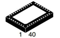
Характеристики

Analog_comparators

2

On_chip_adc

8-chx10-bit

Supplier_package

QFN EP

Specifications

https://4donline.ihs.com/images/VipMasterIC/IC/ONSM/ONSM-S-A0003396939/ONSM-S-A0003396939-1.pdf?hkey=52A5661711E402568146F3353EA87419

Screening_level

Industrial

Schedule_b

8542310000

Ram_size

8.25 KB

Program_memory_type

Flash

Program_memory_size

64 KB

Product_dimensions

7 x 5 x 0.95(Max) mm

Pin_count

40

Operating_temperature

-40 to 85 °C

Operating_supply_voltage

1.8 to 3.6 V

Number_of_timers

5

Бренд

Number_of_programmable_i_os

19

Msl_level

1

Mounting

Surface Mount

Maximum_speed

50 MHz

Max_processing_temp

260 °C

Lead_finish

Gold Over Nickel Palladium

Тип интерфейса

SPI/UART

Instruction_set_architecture

CISC

Htsn

8542310001

Eccn

EAR99

Device_core

8052

Data_bus_width

8 Bit

Watchdog

1

Артикул: AX8052F143-3-TX40

Описание

The AX8052F143 is a true single chip narrow-band, ultra-low power RF-microcontroller SoC for use in licensed and unlicensed bands ranging from 70 MHz to 1050 MHz The on-chip transceiver consists of a fully integrated RF front-end with modulator and demodulator. Base band data processing is implemented in an advanced and flexible communication controller that enables user friendly communication. The AX8052F143 contains a high speed microcontroller compatible to the industry standard 8052 instruction set. It contains 64 Kbytes of FLASH and 8.25 Kbytes of internal SRAM. The AX8052F143 features 3 16-bit general purpose timers with capability, 2 output compare units for generating PWM signals, 2 input compare units to record timings of external signals, 2 16-bit wakeup timers, a watchdog timer, 2 UARTs, a Master/Slave SPI controller, a 10-bit 500 kSample/s A/D converter, 2 analog comparators, a temperature sensor, a 2 channel DMA controller, and a dedicated AES crypto controller. Debugging is aided by a dedicated hardware debug interface controller that connects using a 3-wire protocol (1 dedicated wire, 2 shared with GPIO) to the PC hosting the debug software. While the radio carrier/LO synthesizer can only be clocked by the crystal oscillator (carrier stability requirements dictate a high stability reference clock in the MHz range), the microcontroller and its peripherals provide extremely flexible clocking options. The system clock that clocks the microcontroller, as well as peripheral clocks, can be selected from one of the following clock sources: the crystal oscillator, an internal high speed 20MHz oscillator, an internal low speed 640 Hz/10 kHz oscillator, or the low frequency crystal oscillator. Prescalers offer additional flexibility with their programmable divide by a power of two capability. To improve the accuracy of the internal oscillators, both oscillators may be slaved to the crystal oscillator.

  • SoC Ultra-low Power Advanced Narrow-band RF-microcontroller for Wireless Communication Applications
    • QFN40 Package
    • Supply Range 1.8-3.6V
    • -40°C – 85°C
    • Ultra-low Power Consumption:
      • CPU Active Mode 150A/MHz
    • Sleep Mode with 256Byte RAM Retention and Wake-up Timer running 900nA
      • Radio RX-mode
      • Radio TX-mode at 868MHz

AX8052

  • Ultra-low Power MCU Core Compatible with Industry Standard 8052 Instruction Set
  • Down to 500nA Wake-up Current
  • Single Cycle/Instruction for many Instructions
  • 64 Kbyte In-system Programmable FLASH
  • Code Protection Lock
  • 8.25Kbyte SRAM
  • 3-wire In-circuit Debug Interface Three 16-bit Timers with Output Capability
  • Two 16-bit Wakeup Timers
  • Two Input Captures
  • Two Output Compares with PWM Capability
  • 10-bit 500ksample/s Analog-to-Digital Converter
  • Temperature Sensor
  • Two Analog Comparators
  • Two UARTs
  • One General Purpose Master/Slave SPI
  • Two Channel DMA Controller
  • Multi-megabit/s AES Encryption/Decryption Engine, supports AES-128, AES-192 and AES-256 with True Random Number Generator
  • Ultra-low Power 10kHz/640Hz Wakeup Oscillator, with Automatic Calibration against a Precise Clock
  • Internal 20MHz RC Oscillator, with Automatic Calibration against a Precise Clock for Flexible System Clocking
  • Low Frequency Tuning Fork Crystal Oscillator for Accurate Low Power Time Keeping
  • Brown-out and Power-on-Reset Detection

High Performance Narrow-band RF Transceiver compatible to AX5043

  • Receiver
    • Carrier Frequencies from 27-1050MHz
    • Data Rates from 0.1kbps to 125kbps
    • Optional Forward Error Correction (FEC)
    • Sensitivity without FEC
    • High Selectivity Receiver with up to 47dB Adjacent Channel Rejection
    • 0dBm Maximum Input Power
    • ±10% Data-rate Error Tolerance
    • Support for Antenna Diversity with External Antenna Switch
    • Short Preamble Modes allow the Receiver to work with as little as 16 Preamble Bits
    • Fast State Switching Times
  • Transmitter
    • Carrier Frequencies from 27-1050MHz
    • Data-rates from 0.1kbps to 125kbps
    • High Efficiency, High Linearity Integrated Power Amplifier
    • Maximum Output Power
    • Power Level programmable in 0.5dB Steps
    • GFSK Shaping with BT=0.3 or BT=0.5
    • Unrestricted Power Ramp Shaping
  • RF Frequency Generation
    • Configurable for Usage in 27-1050MHz Bands
    • RF Carrier Frequency and FSK Deviation Programmable in 1 Hz Steps
    • Ultra Fast Settling RF Frequency Synthesizer for Low-power Consumption
    • Fully Integrated RF Frequency Synthesizer with VCO Auto-ranging and Band-width Boost Modes for Fast Locking
    • Configurable for either Fully Integrated VCO, Internal VCO with External Inductor or Fully External VCO
    • Configurable for either Fully Integrated or External Synthesizer Loop Filter for a Large Range of Bandwidths
    • Channel Hopping up to 2000hops/s
    • Automatic Frequency Control
  • Flexible Antenna Interface
    • Integrated RX/TX Switching with Differential Antenna Pins
    • Mode with Differential RX Pins and Single-ended TX Pin
  • Wakeup-on-Radio
    • 640Hz or 10kHz Lowest Power Wake-up Timer
    • Wake-up Time Interval programmable between 98µs and 102s
  • Advanced Crystal Oscillator
    • Fast Start-up and Lowest Power Steady-state XTAL Oscillator for a Wide Range of Crystals
    • Integrated Tuning Capacitors
    • Possibility of Applying an External Clock Reference
Детали

Analog_comparators

2

On_chip_adc

8-chx10-bit

Supplier_package

QFN EP

Specifications

https://4donline.ihs.com/images/VipMasterIC/IC/ONSM/ONSM-S-A0003396939/ONSM-S-A0003396939-1.pdf?hkey=52A5661711E402568146F3353EA87419

Screening_level

Industrial

Schedule_b

8542310000

Ram_size

8.25 KB

Program_memory_type

Flash

Program_memory_size

64 KB

Product_dimensions

7 x 5 x 0.95(Max) mm

Pin_count

40

Operating_temperature

-40 to 85 °C

Operating_supply_voltage

1.8 to 3.6 V

Number_of_timers

5

Бренд

Number_of_programmable_i_os

19

Msl_level

1

Mounting

Surface Mount

Maximum_speed

50 MHz

Max_processing_temp

260 °C

Lead_finish

Gold Over Nickel Palladium

Тип интерфейса

SPI/UART

Instruction_set_architecture

CISC

Htsn

8542310001

Eccn

EAR99

Device_core

8052

Data_bus_width

8 Bit

Watchdog

1