Описание
ATtiny44 is a low-power CMOS 8-bit microcontroller based on the AVR enhanced RISC architecture. By executing powerful instructions in a single clock cycle, the ATtiny44 achieves throughputs approaching 1 MIPS per MHz allowing the system designer to optimize power consumption versus processing speed. The ATtiny44 provides the following features: 4k byte of In-System Programmable Flash, 256 bytes EEPROM, 256 bytes SRAM, 12 general purpose I/O lines, 32 general purpose working registers, an 8-bit Timer/Counter with two PWM channels, a 16-bit timer/counter with two PWM channels, Internal and External Interrupts, a 8-channel 10-bit ADC, programmable gain stage (1x, 20x) for 12 differential ADC channel pairs, a programmable Watchdog Timer with internal oscillator, internal calibrated oscillator, and four software selectable power saving modes. Idle mode stops the CPU while allowing the SRAM, Timer/Counter, ADC, Analog Comparator, and Interrupt system to continue functioning. ADC Noise Reduction mode minimizes switching noise during ADC conversions by stopping the CPU and all I/O modules except the ADC. In Power-down mode registers keep their contents and all chip functions are disabled until the next interrupt or hardware reset. In Standby mode, the crystal/resonator oscillator is running while the rest of the device is sleeping, allowing very fast start-up combined with low power consumption. The device is manufactured using high density non-volatile memory technology. The on chip ISP Flash allows the Program memory to be re-programmed in-system through an SPI serial interface, by a conventional non-volatile memory programmer or by an on-chip boot code running on the AVR core. The ATtiny44 AVR is supported with a full suite of program and system development tools including: C Compilers, Macro Assemblers, Program Debugger/Simulators and Evaluation kits.
- High Performance, Low Power AVR® 8-Bit Microcontroller
- Advanced RISC Architecture
- 120 Powerful Instructions- Most Single Clock Cycle Execution
- 32 x 8 General Purpose Working Registers
- Fully Static Operation
- Non-Volatile Program and Data Memories
- 4 Bytes of In-System Programmable Program Memory Flash
- Endurance: 10,000 Write/Erase Cycles
- 256 Bytes of In-System Programmable EEPROM
- Endurance: 100,000 Write/Erase Cycles
- 256 Bytes of Internal SRAM
- Data Retention: 20 years at 85°C / 100 years at 25°C
- Programming Lock for Self-Programming Flash & EEPROM Data Security
- Peripheral Features
- One 8-Bit and One 16-Bit Timer/Counter with Two PWM Channels, Each
- 10-bit ADC
- 8 Single-Ended Channels
- 12 Differential ADC Channel Pairs with Programmable Gain (1x / 20x)
- Programmable Watchdog Timer with Separate On-chip Oscillator
- On-chip Analog Comparator
- Universal Serial Interface
- Special Microcontroller Features
- debug WIRE On-chip Debug System
- In-System Programmable via SPI Port
- Internal and External Interrupt Sources: Pin Change Interrupt on 12 Pins
- Low Power Idle, ADC Noise Reduction, Standby and Power-Down Modes
- Enhanced Power-on Reset Circuit
- Programmable Brown-out Detection Circuit
- Internal Calibrated Oscillator
- On-chip Temperature Sensor
- I/O and Packages
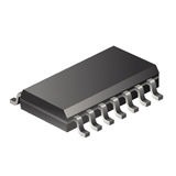
- Available in 20-Pin QFN/MLF & 14-Pin SOIC and PDIP
- Twelve Programmable I/O Lines
- Operating Voltage:
- 1.8 – 5.5V for AT tiny 44V
- Speed Grade AT tiny 44V
- 0 – 4 MHz @ 1.8 – 5.5V
- 0 – 10 MHz @ 2.7 – 5.5V
- Industrial Temperature Range: -40°C to +85°C
- Low Power Consumption
- Active Mode (1 MHz System Clock): 300 µA @ 1.8V
- Power-Down Mode: 0.1 µA @ 1.8V


