Описание
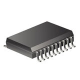
The ATtiny167 is a low-power CMOS 8-bit microcontroller based on the AVR enhanced RISC architecture. By executing powerful instructions in a single clock cycle, the ATtiny167 achieves throughputs approaching 1 MIPS per MHz allowing the system designer to optimize power consumption versus processing speed. The AVR core combines a rich instruction set with 32 general purpose working registers. All the 32 registers are directly connected to the Arithmetic Logic Unit (ALU), allowing two independent registers to be accessed in one single instruction executed in one clock cycle. The resulting architecture is more code efficient while achieving throughputs up to ten times faster than conventional CISC microcontrollers. The ATtiny167 provides the following features: 16K byte of In-System Programmable Flash, 512 bytes SRAM, 32 general purpose working registers, one 8-bit high speed Timer/Counter, Universal Serial Interface, a LIN controller, Internal and External Interrupts, a 11-channel, 10-bit ADC, a programmable Watchdog Timer with internal Oscillator, and three software selectable power saving modes. The Idle mode stops the CPU while allowing the SRAM, Timer/Counter, ADC, Analog Comparator, and Interrupt system to continue functioning. The Power-down mode saves the register contents, disabling all chip functions until the next Interrupt or Hardware Reset. The ADC Noise Reduction mode stops the CPU and all I/O modules except ADC, to minimize switching noise during ADC conversions. The ATtiny167 AVR is supported with a full suite of program and system development tools including: C Compilers, Macro Assemblers, Program Debugger/Simulators, In-Circuit Emulators, and Evaluation kits.
- High Performance, Low Power AVR® 8-bit Microcontroller
- Advanced RISC Architecture
- 123 Powerful Instructions
- Most Single Clock Cycle Execution
- 32 x 8 General Purpose Working Registers
- Fully Static Operation
- Non-volatile Program and Data Memories
- 16K Bytes of In-System Programmable Flash Program Memory
- Endurance: 10,000 Write/Erase Cycles
- 512 Bytes of In-System Programmable EEPROM
- Endurance: 100,000 Write/Erase Cycles
- 512 Bytes of Internal SRAM
- Data retention: 20 Years at 85°C / 100 Years at 25°C
- In-System Programmable via SPI Port
- Low size LIN/UART Software In-System Programmable
- Programming Lock for Software Security
- Peripheral Features
- 1.3 Controller or 8-bit UART
- One 8-bit Asynchronous Timer/Counter with Prescaler
- Output Compare or 8-bit PWM Channel
- One 16-bit Synchronous Timer/Counter with Prescaler
- External Event Counter
- 2 Output Compare Units or PWM Channels each Driving up to 4 Output Pins
- Master/Slave SPI Serial Interface
- Universal Serial Interface with Start Condition Detector
- 10-bit ADC
- 11 Single Ended Channels
- 8 Differential ADC Channel Pairs with Programmable Gain (8x or 20x)
- On-chip Analog Comparator with Selectable Voltage Reference
- 100 µA ±10% Current Source for LIN Node Identification
- On-chip Temperature Sensor
- Programmable Watchdog Timer with Separate On-chip Oscillator
- Special Microcontroller Features
- Software Controlled Clock Switching for Power Control, EMC Reduction
- debugWIRE On-chip Debug System
- External and Internal Interrupt Sources
- Low Power Idle, ADC Noise Reduction, and Power-down Modes
- Power-on Reset and Programmable Brown-out Detection
- Internal 8MHz Calibrated Oscillator
- 4-16 MHz and 32 KHz Crystal/Ceramic Resonator Oscillators
- I/O and Packages
- 16 Programmable I/O Lines
- 20-pin SOIC, 32-pad VQFN and 20-pin TSSOP
- Operating Voltage:
- 1.8 – 5.5V for ATtiny87/167
- Speed Grade:
- 0 – 4 MHz @ 1.8 – 5.5V
- 0 – 8 MHz @ 2.7 – 5.5V
- 0 – 16 MHz @ 4.5 – 5.5V
- Industrial Temperature Range


