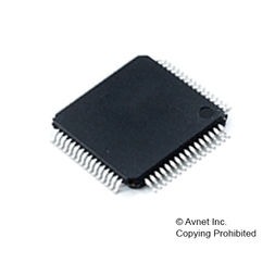
MCU 8-bit ATmega AVR RISC 32KB Flash 3.3V/5V 64-Pin TQFP, ATMEGA325P-20AU, Microchip

The ATmega325P/3250P is a low-power CMOS 8-bit microcontroller based on the AVR enhanced RISC architecture. Byexecuting powerful instructions in a single clock cycle, the ATmega325P/3250P achieves throughputs approaching 1 MIPSper MHz allowing the system designer to optimize power consumption versus processing speed. The AVR core combines a rich instruction set with 32 general purpose working registers. All the32 registers are directly connected to the Arithmetic Logic Unit (ALU), allowing two independentregisters to be accessed in one single instruction executed in one clock cycle. The resultingarchitecture is more code efficient while achieving throughputs up to ten times faster than conventionalCISC microcontrollers. The ATmega325P/3250P provides the following features: 32K bytes of In-System ProgrammableFlash with Read-While-Write capabilities, 1K bytes EEPROM, 2K byte SRAM, 54/69 generalpurpose I/O lines, 32 general purpose working registers, a JTAG interface for Boundary-scan,On-chip Debugging support and programming, three flexible Timer/Counters with comparemodes, internal and external interrupts, a serial programmable USART, Universal Serial Interfacewith Start Condition Detector, an 8-channel, 10-bit ADC, a programmable Watchdog Timerwith internal Oscillator, an SPI serial port, and five software selectable power saving modes. TheIdle mode stops the CPU while allowing the SRAM, Timer/Counters, SPI port, and interrupt systemto continue functioning. The Power-down mode saves the register contents but freezes theOscillator, disabling all other chip functions until the next interrupt or hardware reset. In Powersavemode, the asynchronous timer, allowing the user to maintain a timer base while the rest ofthe device is sleeping. The ADC Noise Reduction mode stops the CPU and all I/O modulesexcept asynchronous timer and ADC, to minimize switching noise during ADC conversions. InStandby mode, the crystal/resonator Oscillator is running while the rest of the device is sleeping.This allows very fast start-up combined with low-power consumption. The device is manufactured using Microchip’s high density non-volatile memory technology. TheOn-chip In-System re-Programmable (ISP) Flash allows the program memory to be reprogrammedIn-System through an SPI serial interface, by a conventional non-volatile memoryprogrammer, or by an On-chip Boot program running on the AVR core. The Boot program canuse any interface to download the application program in the Application Flash memory. Softwarein the Boot Flash section will continue to run while the Application Flash section is updated,providing true Read-While-Write operation. By combining an 8-bit RISC CPU with In-SystemSelf-Programmable Flash on a monolithic chip, the Microchip ATmega325P/3250P is a powerfulmicrocontroller that provides a highly flexible and cost effective solution to many embedded controlapplications. The ATmega325P/3250P AVR is supported with a full suite of program and system developmenttools including: C Compilers, Macro Assemblers, Program Debugger/Simulators, In-CircuitEmulators, and Evaluation kits.

  • High Performance, Low Power AVR® 8-Bit Microcontroller
  • Advanced RISC Architecture
    • 130 Powerful Instructions
    • Most Single Clock Cycle Execution
    • 32 x 8 General Purpose Working Registers
    • Fully Static Operation
    • Up to 20 MIPS Throughput at 20 MHz
    • On-Chip 2-cycle Multiplier
  • High Endurance Non-volatile Memory segments
    • 32K Bytes of In-System Self-programmable Flash program memory
    • 1K Bytes EEPROM
    • 2K Bytes Internal SRAM
    • Write/Erase cyles: 10,000 Flash/100,000 EEPROM
    • Data retention: 20 years at 85°C/100 years at 25°C(1)
    • Optional Boot Code Section with Independent Lock Bits In-System Programming by On-chip Boot Program True Read-While-Write Operation
    • Programming Lock for Software Security
  • JTAG (IEEE std. 1149.1 compliant) Interface
    • Boundary-scan Capabilities According to the JTAG Standard
    • Extensive On-chip Debug Support
    • Programming of Flash, EEPROM, Fuses, and Lock Bits through the JTAG Interface
  • Peripheral Features
    • Two 8-bit Timer/Counters with Separate Prescaler and Compare Mode
    • One 16-bit Timer/Counter with Separate Prescaler, Compare Mode, and Capture Mode
    • Real Time Counter with Separate Oscillator
    • Four PWM Channels
    • 8-channel, 10-bit ADC
    • Programmable Serial USART
    • Master/Slave SPI Serial Interface
    • Universal Serial Interface with Start Condition Detector
    • Programmable Watchdog Timer with Separate On-chip Oscillator
    • On-chip Analog Comparator
    • Interrupt and Wake-up on Pin Change
  • Special Microcontroller Features
    • Power-on Reset and Programmable Brown-out Detection
    • Internal Calibrated Oscillator
    • External and Internal Interrupt Sources
    • Five Sleep Modes: Idle, ADC Noise Reduction, Power-save, Power-down, and Standby
  • I/O and Packages
    • 54/69 Programmable I/O Lines
    • 64-lead TQFP, 64-pad QFN/MLF, and 100-lead TQFP
  • Speed Grade:
    • ATmega325PV/ATmega3250PV: 0 – 4 MHz @ 1.8 – 5.5V, 0 – 10 MHz @ 2.7 – 5.5V
    • ATmega325P/3250P: 0 – 10 MHz @ 2.7 – 5.5V, 0 – 20 MHz @ 4.5 – 5.5V
  • Temperature range:
    • -40°C to 85°C Industrial
  • Ultra-Low Power Consumption
    • Active Mode: 420 µA at 1 MHz, 1.8V
    • Power-down Mode: 40 nA at 1.8V
    • Power-save Mode: 750 nA at 1.8V

Характеристики

Analog_comparators

1

On_chip_adc

8-chx10-bit

Max_operating_supply_voltage

5.5 V

Watchdog

1

Supplier_package

TQFP

Specifications

https://4donline.ihs.com/images/VipMasterIC/IC/ATML/ATMLS05255/ATMLS05255-1.pdf?hkey=52A5661711E402568146F3353EA87419

Screening_level

Industrial

Schedule_b

8542390000

Ram_size

2 KB

Program_memory_type

Flash

Program_memory_size

32 Kb

Product_dimensions

14.1 x 14.1 x 1.05 mm

Pin_count

64

Operating_temperature

-40 to 85 °C

Operating_supply_voltage

3.3, 5 V

Number_of_timers

3

Бренд

Number_of_programmable_i_os

54

Msl_level

3

Mounting

Surface Mount

Maximum_speed

20 MHz

Max_processing_temp

260

Lead_finish

Matte Tin

Тип интерфейса

SPI/USART/USI

Instruction_set_architecture

RISC

Htsn

8542310001

Eccn

EAR99

Device_core

AVR

Data_bus_width

8 Bit

Country_of_origin

Taiwan

Min_operating_supply_voltage

2.7 V

Артикул: ATMEGA325P-20AU

Описание

The ATmega325P/3250P is a low-power CMOS 8-bit microcontroller based on the AVR enhanced RISC architecture. Byexecuting powerful instructions in a single clock cycle, the ATmega325P/3250P achieves throughputs approaching 1 MIPSper MHz allowing the system designer to optimize power consumption versus processing speed. The AVR core combines a rich instruction set with 32 general purpose working registers. All the32 registers are directly connected to the Arithmetic Logic Unit (ALU), allowing two independentregisters to be accessed in one single instruction executed in one clock cycle. The resultingarchitecture is more code efficient while achieving throughputs up to ten times faster than conventionalCISC microcontrollers. The ATmega325P/3250P provides the following features: 32K bytes of In-System ProgrammableFlash with Read-While-Write capabilities, 1K bytes EEPROM, 2K byte SRAM, 54/69 generalpurpose I/O lines, 32 general purpose working registers, a JTAG interface for Boundary-scan,On-chip Debugging support and programming, three flexible Timer/Counters with comparemodes, internal and external interrupts, a serial programmable USART, Universal Serial Interfacewith Start Condition Detector, an 8-channel, 10-bit ADC, a programmable Watchdog Timerwith internal Oscillator, an SPI serial port, and five software selectable power saving modes. TheIdle mode stops the CPU while allowing the SRAM, Timer/Counters, SPI port, and interrupt systemto continue functioning. The Power-down mode saves the register contents but freezes theOscillator, disabling all other chip functions until the next interrupt or hardware reset. In Powersavemode, the asynchronous timer, allowing the user to maintain a timer base while the rest ofthe device is sleeping. The ADC Noise Reduction mode stops the CPU and all I/O modulesexcept asynchronous timer and ADC, to minimize switching noise during ADC conversions. InStandby mode, the crystal/resonator Oscillator is running while the rest of the device is sleeping.This allows very fast start-up combined with low-power consumption. The device is manufactured using Microchip’s high density non-volatile memory technology. TheOn-chip In-System re-Programmable (ISP) Flash allows the program memory to be reprogrammedIn-System through an SPI serial interface, by a conventional non-volatile memoryprogrammer, or by an On-chip Boot program running on the AVR core. The Boot program canuse any interface to download the application program in the Application Flash memory. Softwarein the Boot Flash section will continue to run while the Application Flash section is updated,providing true Read-While-Write operation. By combining an 8-bit RISC CPU with In-SystemSelf-Programmable Flash on a monolithic chip, the Microchip ATmega325P/3250P is a powerfulmicrocontroller that provides a highly flexible and cost effective solution to many embedded controlapplications. The ATmega325P/3250P AVR is supported with a full suite of program and system developmenttools including: C Compilers, Macro Assemblers, Program Debugger/Simulators, In-CircuitEmulators, and Evaluation kits.

  • High Performance, Low Power AVR® 8-Bit Microcontroller
  • Advanced RISC Architecture
    • 130 Powerful Instructions
    • Most Single Clock Cycle Execution
    • 32 x 8 General Purpose Working Registers
    • Fully Static Operation
    • Up to 20 MIPS Throughput at 20 MHz
    • On-Chip 2-cycle Multiplier
  • High Endurance Non-volatile Memory segments
    • 32K Bytes of In-System Self-programmable Flash program memory
    • 1K Bytes EEPROM
    • 2K Bytes Internal SRAM
    • Write/Erase cyles: 10,000 Flash/100,000 EEPROM
    • Data retention: 20 years at 85°C/100 years at 25°C(1)
    • Optional Boot Code Section with Independent Lock Bits In-System Programming by On-chip Boot Program True Read-While-Write Operation
    • Programming Lock for Software Security
  • JTAG (IEEE std. 1149.1 compliant) Interface
    • Boundary-scan Capabilities According to the JTAG Standard
    • Extensive On-chip Debug Support
    • Programming of Flash, EEPROM, Fuses, and Lock Bits through the JTAG Interface
  • Peripheral Features
    • Two 8-bit Timer/Counters with Separate Prescaler and Compare Mode
    • One 16-bit Timer/Counter with Separate Prescaler, Compare Mode, and Capture Mode
    • Real Time Counter with Separate Oscillator
    • Four PWM Channels
    • 8-channel, 10-bit ADC
    • Programmable Serial USART
    • Master/Slave SPI Serial Interface
    • Universal Serial Interface with Start Condition Detector
    • Programmable Watchdog Timer with Separate On-chip Oscillator
    • On-chip Analog Comparator
    • Interrupt and Wake-up on Pin Change
  • Special Microcontroller Features
    • Power-on Reset and Programmable Brown-out Detection
    • Internal Calibrated Oscillator
    • External and Internal Interrupt Sources
    • Five Sleep Modes: Idle, ADC Noise Reduction, Power-save, Power-down, and Standby
  • I/O and Packages
    • 54/69 Programmable I/O Lines
    • 64-lead TQFP, 64-pad QFN/MLF, and 100-lead TQFP
  • Speed Grade:
    • ATmega325PV/ATmega3250PV: 0 – 4 MHz @ 1.8 – 5.5V, 0 – 10 MHz @ 2.7 – 5.5V
    • ATmega325P/3250P: 0 – 10 MHz @ 2.7 – 5.5V, 0 – 20 MHz @ 4.5 – 5.5V
  • Temperature range:
    • -40°C to 85°C Industrial
  • Ultra-Low Power Consumption
    • Active Mode: 420 µA at 1 MHz, 1.8V
    • Power-down Mode: 40 nA at 1.8V
    • Power-save Mode: 750 nA at 1.8V

Детали

Analog_comparators

1

On_chip_adc

8-chx10-bit

Max_operating_supply_voltage

5.5 V

Watchdog

1

Supplier_package

TQFP

Specifications

https://4donline.ihs.com/images/VipMasterIC/IC/ATML/ATMLS05255/ATMLS05255-1.pdf?hkey=52A5661711E402568146F3353EA87419

Screening_level

Industrial

Schedule_b

8542390000

Ram_size

2 KB

Program_memory_type

Flash

Program_memory_size

32 Kb

Product_dimensions

14.1 x 14.1 x 1.05 mm

Pin_count

64

Operating_temperature

-40 to 85 °C

Operating_supply_voltage

3.3, 5 V

Number_of_timers

3

Бренд

Number_of_programmable_i_os

54

Msl_level

3

Mounting

Surface Mount

Maximum_speed

20 MHz

Max_processing_temp

260

Lead_finish

Matte Tin

Тип интерфейса

SPI/USART/USI

Instruction_set_architecture

RISC

Htsn

8542310001

Eccn

EAR99

Device_core

AVR

Data_bus_width

8 Bit

Country_of_origin

Taiwan

Min_operating_supply_voltage

2.7 V