Описание
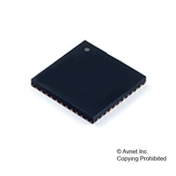
The ATmega32U4 is a low-power CMOS 8-bit microcontroller based on the AVR enhanced RISCarchitecture. By executing powerful instructions in a single clock cycle, the device achieves throughputsapproaching 1 MIPS per MHz allowing the system designer to optimize power consumption versus processingspeed. The AVR core combines a rich instruction set with 32 general purpose working registers. All the 32 registers aredirectly connected to the Arithmetic Logic Unit (ALU), allowing two independent registers to be accessed in onesingle instruction executed in one clock cycle. The resulting architecture is more code efficient while achievingthroughputs up to ten times faster than conventional CISC microcontrollers. The device provides the following features: 16/32K bytes of In-System Programmable Flash with Read-WhileWritecapabilities, 512Bytes/1K bytes EEPROM, 1.25/2.5K bytes SRAM, 26 general purpose I/O lines (CMOSoutputs and LVTTL inputs), 32 general purpose working registers, four flexible Timer/Counters with comparemodes and PWM, one more high-speed Timer/Counter with compare modes and PLL adjustable source, oneUSART (including CTS/RTS flow control signals), a byte oriented 2-wire Serial Interface, a 12-channels 10-bitADC with optional differential input stage with programmable gain, an on-chip calibrated temperature sensor, aprogrammable Watchdog Timer with Internal Oscillator, an SPI serial port, IEEE std. 1149.1 compliant JTAGtest interface, also used for accessing the On-chip Debug system and programming and six software selectablepower saving modes. The Idle mode stops the CPU while allowing the SRAM, Timer/Counters, SPI port, andinterrupt system to continue functioning. The Power-down mode saves the register contents but freezes theOscillator, disabling all other chip functions until the next interrupt or Hardware Reset. The ADC NoiseReduction mode stops the CPU and all I/O modules except ADC, to minimize switching noise during ADCconversions. In Standby mode, the Crystal/Resonator Oscillator is running while the rest of the device issleeping. This allows very fast start-up combined with low power consumption. The device is manufactured using the Microchip high-density nonvolatile memory technology. The On-chip ISPFlash allows the program memory to be reprogrammed in-system through an SPI serial interface, by aconventional nonvolatile memory programmer, or by an On-chip Boot program running on the AVR core. Theboot program can use any interface to download the application program in the application Flash memory.Software in the Boot Flash section will continue to run while the Application Flash section is updated, providingtrue Read-While-Write operation. By combining an 8-bit RISC CPU with In-System Self-Programmable Flash ona monolithic chip, the device is a powerful microcontroller that provides a highly flexible and cost effectivesolution to many embedded control applications. The ATmega32U4 AVR is supported with a full suite of program and system development toolsincluding: C compilers, macro assemblers, program debugger/simulators, in-circuit emulators, and evaluationkits.
- High Performance, Low Power AVR® 8-Bit Microcontroller
- Advanced RISC Architecture
- 135 Powerful Instructions
- Most Single Clock Cycle Execution
- 32 x 8 General Purpose Working Registers
- Fully Static Operation
- Up to 16 MIPS Throughput at 16MHz
- On-Chip 2-cycle Multiplier
- Non-volatile Program and Data Memories
- 16/32KB of In-System Self-Programmable Flash
- 1.25/2.5KB Internal SRAM
- 512Bytes/1KB Internal EEPROM
- Write/Erase Cycles: 10,000 Flash/100,000 EEPROM
- Data retention: 20 years at 85°C/ 100 years at 25°C(1)
- Optional Boot Code Section with Independent Lock Bits In-System Programming by On-chip Boot Program True Read-While-Write Operation Parts using external XTAL clock are pre-programed with a default USB bootloader
- Programming Lock for Software Security
- JTAG (IEEE® std. 1149.1 compliant) Interface
- Boundary-scan Capabilities According to the JTAG Standard
- Extensive On-chip Debug Support
- Programming of Flash, EEPROM, Fuses, and Lock Bits through the JTAG Interface
- USB 2.0 Full-speed/Low Speed Device Module with Interrupt on Transfer Completion
- Complies fully with Universal Serial Bus Specification Rev 2.0
- Supports data transfer rates up to 12Mbit/s and 1.5Mbit/s
- Endpoint 0 for Control Transfers: up to 64-bytes
- Six Programmable Endpoints with IN or Out Directions and with Bulk, Interrupt or Isochronous Transfers
- Configurable Endpoints size up to 256 bytes in double bank mode
- Fully independent 832 bytes USB DPRAM for endpoint memory allocation
- Suspend/Resume Interrupts
- CPU Reset possible on USB Bus Reset detection
- 48MHz from PLL for Full-speed Bus Operation
- USB Bus Connection/Disconnection on Microcontroller Request
- Crystal-less operation for Low Speed mode
- Peripheral Features
- On-chip PLL for USB and High Speed Timer: 32 up to 96MHz operation
- One 8-bit Timer/Counter with Separate Prescaler and Compare Mode
- Two 16-bit Timer/Counter with Separate Prescaler, Compare- and Capture Mode
- One 10-bit High-Speed Timer/Counter with PLL (64MHz) and Compare Mode
- Four 8-bit PWM Channels
- Four PWM Channels with Programmable Resolution from 2 to 16 Bits
- Six PWM Channels for High Speed Operation, with Programmable Resolution from 2 to 11 Bits
- Output Compare Modulator
- 12-channels, 10-bit ADC (features Differential Channels with Programmable Gain)
- Programmable Serial USART with Hardware Flow Control
- Master/Slave SPI Serial Interface
- Byte Oriented 2-wire Serial Interface
- Programmable Watchdog Timer with Separate On-chip Oscillator
- On-chip Analog Comparator
- Interrupt and Wake-up on Pin Change
- On-chip Temperature Sensor
- Special Microcontroller Features
- Power-on Reset and Programmable Brown-out Detection
- Internal 8MHz Calibrated Oscillator
- External and Internal Interrupt Sources
- Six Sleep Modes: Idle, ADC Noise Reduction, Power-save, Power-down, Standby, and Extended Standby
- I/O and Packages
- All I/O combine CMOS outputs and LVTTL inputs
- 26 Programmable I/O Lines
- 44-lead TQFP Package, 10x10mm
- 44-lead QFN Package, 7x7mm
- Operating Voltages
- 2.7 – 5.5V
- Operating temperature
- Industrial (-40°C to +85°C)
- Maximum Frequency
- 8MHz at 2.7V – Industrial range
- 16MHz at 4.5V – Industrial range
