Описание
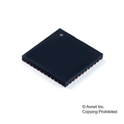
The AVR XMEGA is a family of low power, high performance, and peripheral rich 8/16-bit microcontrollers based on the AVR enhanced RISC architecture. By executing instructions in a single clock cycle, the AVR XMEGA device achieves throughputs CPU approaching one million instructions per second (MIPS) per megahertz, allowing the system designer to optimize power consumption versus processing speed. The AVR CPU combines a rich instruction set with 32 general purpose working registers. All 32 registers are directly connected to the arithmetic logic unit (ALU), allowing two independent registers to be accessed in a single instruction, executed in one clock cycle. The resulting architecture is more code efficient while achieving throughputs many times faster than conventional single-accumulator or CISC based microcontrollers. The AVR XMEGA A3U devices provide the following features: in-system programmable flash with read-while write capabilities; internal EEPROM and SRAM; four-channel DMA controller, eight-channel event system and programmable multilevel interrupt controller, 50 general purpose I/O lines, 16-bit real-time counter (RTC); seven flexible, 16-bit timer/counters with compare and PWM channels; seven USARTs; two two-wire serial interfaces (TWIs); one full speed USB 2.0 interface; three serial peripheral interfaces (SPIs); AES and DES cryptographic engine; two 16-channel, 12-bit ADCs with programmable gain; one 2-channel 12-bit DAC; four analog comparators (ACs) with window mode; programmable watchdog timer with separate internal oscillator; accurate internal oscillators with PLL and presale; and programmable brown-out detection.
- High-performance, low-power 8-bit Microcontroller
- Advanced RISC architecture
- 131 powerful Instructions – most single-clock cycle execution
- 32 × 8 general purpose working registers
- Fully static operation
- Up to 20MIPS throughput at 20MHz
- On-chip 2-cycle multiplier
- High endurance non-volatile memory segments
- 16Kbytes of In-System Self-programmable Flash program memory
- 512bytes EEPROM
- 1Kbytes Internal SRAM
- Write/Erase Cycles: 10,000 Flash/ 100,000 EEPROM
- Data retention: 20 years at 85°C/ 100 years at 25°C(1)
- Optional Boot Code Section with Independent Lock Bits
- In-System Programming by On-chip Boot Program
- True Read-While-Write Operation
- Programming Lock for Software Security
- QTouch® library support
- Capacitive touch buttons, sliders and wheels
- QTouch and QMatrix acquisition
- Up to 64 sense channels
- JTAG (IEEE std. 1149.1 Compliant) Interface
- Boundary-scan Capabilities According to the JTAG Standard
- Extensive On-chip Debug Support
- Programming of Flash, EEPROM, Fuses, and Lock Bits through the JTAG Interface
- Peripheral Features
- Two 8-bit Timer/Counters with Separate Prescalers and Compare Modes
- One/two 16-bit Timer/Counter with Separate Prescaler, Compare Mode, and Capture Mode
- Real Time Counter with Separate Oscillator
- Six PWM Channels
- 8-channel, 10-bit ADC
- Differential mode with selectable gain at 1×, 10× or 200×
- Byte-oriented Two-wire Serial Interface
- Two Programmable Serial USART
- Master/Slave SPI Serial Interface


