Описание
The AT89LP216 is a low-power, high-performance CMOS 8-bit microcontroller with 2K bytes of In-System Programmable Flash memory. The device is manufactured using Microchip "s high-density nonvolatile memory technology and is compatible with the industry-standard MCS-51 instruction set. The AT89LP216 is built around an enhanced CPU core that can fetch a single byte from memory every clock cycle. In the classic 8051 architecture, each fetch requires 6 clock cycles, forcing instructions to execute in 12, 24 or 48 clock cycles. In the AT89LP216 CPU, instructions need only 1 to 4 clock cycles providing 6 to 12 times more throughput than the standard 8051. Seventy percent of instructions need only as many clock cycles as they have bytes to execute, and most of the remaining instructions require only one additional clock. The enhanced CPU core is capable of 20 MIPS throughput whereas the classic 8051 CPU can deliver only 4 MIPS at the same current consumption. Conversely, at the same throughput as the classic 8051, the new CPU core runs at a much lower speed and thereby greatly reduces power consumption. need only 1 to 4 clock cycles providing 6 to 12 times more throughput than the standard 8051. Seventy percent of instructions need only as many clock cycles as they have bytes to execute, and most of the remaining instructions require only one additional clock. The enhanced CPU core is capable of 20 MIPS throughput whereas the classic 8051 CPU can deliver only 4 MIPS at the same current consumption. Conversely, at the same throughput as the classic 8051, the new CPU core runs at a much lower speed and thereby greatly reduces power consumption. The two timer/counters in the AT89LP216 are enhanced with two new modes. Mode 0 can be configured as a variable 9- to 16-bit timer/counter and Mode 1 can be configured as a 16-bit auto-reload timer/counter. In addition, the timer/counters may independently drive a pulse width modulation output.
- 8-bit Microcontroller Compatible with MCS®51 Products
- Enhanced 8051 Architecture
- Single Clock Cycle per Byte Fetch
- Up to 20 MIPS Throughput at 20 MHz Clock Frequency
- Fully Static Operation: 0 Hz to 20 MHz
- On-chip 2-cycle Hardware Multiplier
- 128 x 8 Internal RAM
- 4-level Interrupt Priority
- Nonvolatile Program Memory
- 2K Bytes of In-System Programmable (ISP) Flash Memory
- Endurance: Minimum 10,000 Write/Erase Cycles
- Serial Interface for Program Downloading
- 32-byte Fasts Programming Mode
- 64-byte User Signature Array
- 2-level Program Memory Lock for Software Security
- Peripheral Features
- Two 16-bit Enhanced Timer/Counters
- Two 8-bit PWM Outputs
- Enhanced UART with Automatic Address Recognition and Framing Error Detection
- Enhanced Master/Slave SPI with Double-buffered Send/Receive
- Programmable Watchdog Timer with Software Reset
- Analog Comparator with Selectable Interrupt and Debouncing
- 8 General-purpose Interrupt Pins
- Special Microcontroller Features
- Two-wire On-chip Debug Interface
- Brown-out Detection and Power-on Reset with Power-off Flag
- Internal 8 MHz RC Oscillator
- Low Power Idle and Power-down Modes
- Interrupt Recovery from Power-down Mode
- I/O and Packages
- Up to 14 Programmable I/O Lines
- Configurable I/O with Quasi-bidirectional, Input, Push-pull Output, and Open-drain Modes
- 5V Tolerant I/O
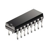
- 16-lead TSSOP, SOIC or PDIP
- Operating Conditions
- 2.4V to 5.5V VCC Voltage Range
- -40· C to 85°C Temperature Range


