Описание
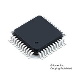
The MB95F698K is a series of general-purpose, single-chip microcontrollers. In addition to a compact instruction set, the microcontrollers of this series contain a variety of peripheral functions.
- F2MC-8FX CPU core Instruction set optimized for controllers
- Multiplication and division instructions
- 16-bit arithmetic operations
- Bit test branch instructions
- Bit manipulation instructions, etc. Note: F2MC is the abbreviation of FUJITSU Flexible Microcontroller.
- Clock
- Selectable main clock source
- Main oscillation clock (up to 16.25 MHz, maximum machine clock frequency: 8.125 MHz)
- External clock (up to 32.5 MHz, maximum machine clock frequency: 16.25 MHz)
- Main CR clock (4 MHz ±2%)
- Main CR PLL clock
- The main CR PLL clock frequency becomes 8 MHz ±2% when the PLL multiplication rate is 2.
- The main CR PLL clock frequency becomes 10 MHz ±2% when the PLL multiplication rate is 2.5.
- The main CR PLL clock frequency becomes 12 MHz ±2% when the PLL multiplication rate is 3.
- The main CR PLL clock frequency becomes 16 MHz ±2% when the PLL multiplication rate is 4.
- Selectable subclock source
- Suboscillation clock (32.768 kHz)
- External clock (32.768 kHz)
- Sub-CR clock (Typ: 100 kHz, Min: 50 kHz, Max: 150 kHz)
- Timer
- 8/16-bit composite timer × 2 channels
- 8/16-bit PPG × 3 channels
- 16-bit PPG timer × 1 channel (can work independently or together with the multi-pulse generator)
- 16-bit reload timer × 1 channel (can work independently or together with the multi-pulse generator)
- Time-base timer × 1 channel
- Watch prescaler × 1 channel
- UART/SIO × 1 channel
- Full duplex double buffer
- Capable of clock asynchronous (UART) serial data transfer and clock synchronous (SIO) serial data transfer
- I2C bus interface × 1 channel Built-in wake-up function
- Multi-pulse generator (MPG) (for DC motor control) × 1 channel
- 16-bit reload timer × 1 channel
- 16-bit PPG timer × 1 channel
- Waveform sequencer (including a 16-bit timer equipped with a buffer and a compare clear function)
- LIN-UART
- Full duplex double buffer
- Capable of clock asynchronous serial data transfer and clock synchronous serial data transfer
- External interrupt There are four standby modes as follows:
- Stop mode
- Sleep mode
- Watch mode
- Time-base timer mode In standby mode, two further options can be selected: normal standby mode and deep standby mode.
- I/O port On-chip debug
- 1-wire serial control
- Serial writing supported (asynchronous mode)
- Hardware/software watchdog timer
- Built-in hardware watchdog timer
- Built-in software watchdog timer
- Power-on reset A power-on reset is generated when the power is switched on.
- Low-voltage detection (LVD) reset circuit
- The LVD function is enabled by default.
- The LVD function can be controlled through software.
- The LVD reset circuit control register (LVDCC) enables or disables the LVD reset.
- The LVD reset circuit has an internal low-voltage detector. The combination of detection voltage and release voltage can be selected from four options.
- Comparator × 2 channels
- Built-in dedicated BGR
- The comparator reference voltage can be selected between the BGR voltage and the comparator pin.
- Clock supervisor counter Built-in clock supervisor counter
- Dual operation Flash memory The program/erase operation and the read operation can be executed in different banks (upper bank/lower bank) simultaneously.
- Flash memory security function Protects the content of the Flash memory.