Описание
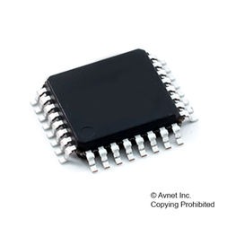
The MB95F634K is a series of general-purpose, single-chip microcontrollers. In addition to a compact instruction set, the microcontrollers of this series contain a variety of peripheral functions.
- F2MC-8FX CPU core Instruction set optimized for controllers
- Multiplication and division instructions
- 16-bit arithmetic operations
- Bit test branch instructions
- Bit manipulation instructions, etc. Note: F2MC is the abbreviation of FUJITSU Flexible Microcontroller.
- Clock
- Selectable main clock source
- Main oscillation clock (up to 16.25 MHz, maximum machine clock frequency: 8.125 MHz)
- External clock (up to 32.5 MHz, maximum machine clock frequency: 16.25 MHz)
- Main CR clock (4 MHz ±2%)
- Main CR PLL clock
- The main CR PLL clock frequency becomes 8 MHz ±2% when the PLL multiplication rate is 2.
- The main CR PLL clock frequency becomes 10 MHz ±2% when the PLL multiplication rate is 2.5.
- The main CR PLL clock frequency becomes 12 MHz ±2% when the PLL multiplication rate is 3.
- The main CR PLL clock frequency becomes 16 MHz ±2% when the PLL multiplication rate is 4.
- Selectable subclock source
- Suboscillation clock (32.768 kHz)
- External clock (32.768 kHz)
- Sub-CR clock (Typ: 100 kHz, Min: 50 kHz, Max: 150 kHz)
- Timer
- 8/16-bit composite timer – 2 channels
- 8/16-bit PPG – 3 channels
- 16-bit PPG timer – 1 channel (can work independently or together with the multi-pulse generator)
- 16-bit reload timer – 1 channel (can work independently or together with the multi-pulse generator)
- Time-base timer – 1 channel
- Watch prescaler – 1 channel
- UART/SIO – 1 channel
- Full duplex double buffer
- Capable of clock asynchronous (UART) serial data transfer and clock synchronous (SIO) serial data transfer
- I2C bus interface – 1 channel Built-in wake-up function
- Multi-pulse generator (MPG) (for DC motor control) – 1 channel
- 16-bit reload timer – 1 channel
- 16-bit PPG timer – 1 channel
- Waveform sequencer (including a 16-bit timer equipped with a buffer and a compare clear function)
- LIN-UART
- Full duplex double buffer
- Capable of clock asynchronous serial data transfer and clock synchronous serial data transfer
- External interrupt – 10 channels
- Interrupt by edge detection (rising edge, falling edge, and both edges can be selected)
- Can be used to wake up the device from different low power consumption (standby) modes
- 8/10-bit A/D converter – 8 channels
- 8-bit or 10-bit resolution can be selected.
- Low power consumption (standby) modes There are four standby modes as follows:
- Stop mode
- Sleep mode
- Watch mode
- Time-base timer mode In standby mode, two further options can be selected: normal standby mode and deep standby mode.
- I/O port
- Number of I/O ports: 29
- General-purpose I/O ports (CMOS I/O) : 25
- General-purpose I/O ports (N-ch open drain) : 3