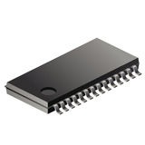
MCU 8-bit 89LP 80C51 CISC 4KB Flash 2.5V/3.3V 28-Pin TSSOP, P89LPC930FDH,129, NXP

The P89LPC930/931 are single-chip microcontrollers designed for applications demanding high-integration, low cost solutions over a wide range of performance requirements. The P89LPC930/931 is based on a high performance processor architecture that executes instructions in two to four clocks, six times the rate of standard 80C51 devices. Many system-level functions have been incorporated into the P89LPC930/931 in order to reduce component count, board space, and system cost.

  • A high performance 80C51 CPU provides instruction cycle times of 111 ns to 222 ns for all instructions except multiply and divide when executing at 18 MHz. This is 6 times the performance of the standard 80C51 running at the same clock frequency. A lower clock frequency for the same performance results in power savings and reduced EMI.
  • 2.4 V to 3.6 V VDD operating range. I/O pins are 5 V tolerant (may be pulled up or driven to 5.5 V).
  • 4 KB Flash code memory with 1 KB sectors, and 64-byte page size.
  • Byte-erase allowing code memory to be used for data storage.
  • Flash program operation completes in 2 ms.
  • Flash erase operation completes in 2 ms.
  • 256-byte RAM data memory.
  • Two 16-bit counter/timers. Each timer may be configured to toggle a port output upon timer overflow or to become a PWM output.
  • Real-Time clock that can also be used as a system timer.
  • Two analog comparators with selectable inputs and reference source.
  • Enhanced UART with fractional baud rate generator, break detect, framing error detection, automatic address detection and versatile interrupt capabilities.
  • 400 kHz byte-wide I²C-bus communication port.
  • SPI communication port.
  • Eight keypad interrupt inputs, plus two additional external interrupt inputs.
  • Four interrupt priority levels.
  • Watchdog timer with separate on-chip oscillator, requiring no external components. The Watchdog time-out time is selectable from 8 values.
  • Active-LOW reset. On-chip power-on reset allows operation without external reset components. A reset counter and reset glitch suppression circuitry prevent spurious and incomplete resets. A software reset function is also available.
  • Low voltage reset (Brownout detect) allows a graceful system shutdown when power fails. May optionally be configured as an interrupt.
  • Oscillator Fail Detect. The watchdog timer has a separate fully on-chip oscillator allowing it to perform an oscillator fail detect function.
  • Configurable on-chip oscillator with frequency range and RC oscillator options (selected by user programmed Flash configuration bits). The RC oscillator (factory calibrated to +-1 pct) option allows operation without external oscillator components. Oscillator options support frequencies from 20 kHz to the maximum operating frequency of 18 MHz. The RC oscillator option is selectable and fine tunable.
  • Programmable port output configuration options:
    • Quasi-bidirectional
    • Open drain
    • Push-pull
    • Input-only
  • Port "input pattern match detect. Port 0 may generate an interrupt when the value of the pins match or do not match a programmable pattern.
  • Second data pointer.
  • Schmitt trigger port inputs.
  • LED drive capability (20 mA) on all port pins. Maximum combined I/O current of 100 mA.
  • Controlled slew rate port outputs to reduce EMI. Outputs have approximately 10 ns minimum ramp times.
  • 23 I/O pins minimum (28-pin package). Up to 26 I/O pins while using on-chip oscillator and reset options.
  • Only power and ground connections are required to operate the P89LPC930/931 using on-chip oscillator and on-chip reset options.
  • Serial Flash programming allows in-circuit production coding. Flash security bits prevent reading of sensitive programs.
  • In-Application Programming of the Flash code memory. This allows changing the code in a running application.
  • Idle and two different Power-down reduced power modes Typical Power-down current is 1 uA (total Power-down with voltage comparators disabled).
  • 28-pin TSSOP package.
  • Emulation support.

Характеристики

Бренд

Operating_supply_voltage

2.5, 3.3 V

Max_power_dissipation

1500 mW

Min_operating_supply_voltage

2.4 V

Max_operating_supply_voltage

3.6 V

Supplier_package

TSSOP

Specifications

https://4donline.ihs.com/images/VipMasterIC/IC/PHGL/PHGLS13361/PHGLS13361-1.pdf?hkey=52A5661711E402568146F3353EA87419

Screening_level

Industrial

Schedule_b

8542390000

Ram_size

256 byte

Program_memory_type

Flash

Program_memory_size

4 Kb

Product_dimensions

9.8 x 4.5 x 0.95 mm

Pin_count

28

Operating_temperature

-40 to 85 °C

Number_of_timers

2

Country_of_origin

United States

Number_of_programmable_i_os

26

Msl_level

1

Mounting

Surface Mount

Maximum_speed

18 MHz

Max_processing_temp

260

Lead_finish

Gold

Тип интерфейса

I2C/SPI/UART

Instruction_set_architecture

CISC

Htsn

8542310001

Eccn

EAR99

Device_core

80C51

Data_bus_width

8 Bit

Max_expanded_memory_size

64 KB

Артикул: P89LPC930FDH,129

Описание

The P89LPC930/931 are single-chip microcontrollers designed for applications demanding high-integration, low cost solutions over a wide range of performance requirements. The P89LPC930/931 is based on a high performance processor architecture that executes instructions in two to four clocks, six times the rate of standard 80C51 devices. Many system-level functions have been incorporated into the P89LPC930/931 in order to reduce component count, board space, and system cost.

  • A high performance 80C51 CPU provides instruction cycle times of 111 ns to 222 ns for all instructions except multiply and divide when executing at 18 MHz. This is 6 times the performance of the standard 80C51 running at the same clock frequency. A lower clock frequency for the same performance results in power savings and reduced EMI.
  • 2.4 V to 3.6 V VDD operating range. I/O pins are 5 V tolerant (may be pulled up or driven to 5.5 V).
  • 4 KB Flash code memory with 1 KB sectors, and 64-byte page size.
  • Byte-erase allowing code memory to be used for data storage.
  • Flash program operation completes in 2 ms.
  • Flash erase operation completes in 2 ms.
  • 256-byte RAM data memory.
  • Two 16-bit counter/timers. Each timer may be configured to toggle a port output upon timer overflow or to become a PWM output.
  • Real-Time clock that can also be used as a system timer.
  • Two analog comparators with selectable inputs and reference source.
  • Enhanced UART with fractional baud rate generator, break detect, framing error detection, automatic address detection and versatile interrupt capabilities.
  • 400 kHz byte-wide I²C-bus communication port.
  • SPI communication port.
  • Eight keypad interrupt inputs, plus two additional external interrupt inputs.
  • Four interrupt priority levels.
  • Watchdog timer with separate on-chip oscillator, requiring no external components. The Watchdog time-out time is selectable from 8 values.
  • Active-LOW reset. On-chip power-on reset allows operation without external reset components. A reset counter and reset glitch suppression circuitry prevent spurious and incomplete resets. A software reset function is also available.
  • Low voltage reset (Brownout detect) allows a graceful system shutdown when power fails. May optionally be configured as an interrupt.
  • Oscillator Fail Detect. The watchdog timer has a separate fully on-chip oscillator allowing it to perform an oscillator fail detect function.
  • Configurable on-chip oscillator with frequency range and RC oscillator options (selected by user programmed Flash configuration bits). The RC oscillator (factory calibrated to +-1 pct) option allows operation without external oscillator components. Oscillator options support frequencies from 20 kHz to the maximum operating frequency of 18 MHz. The RC oscillator option is selectable and fine tunable.
  • Programmable port output configuration options:
    • Quasi-bidirectional
    • Open drain
    • Push-pull
    • Input-only
  • Port "input pattern match detect. Port 0 may generate an interrupt when the value of the pins match or do not match a programmable pattern.
  • Second data pointer.
  • Schmitt trigger port inputs.
  • LED drive capability (20 mA) on all port pins. Maximum combined I/O current of 100 mA.
  • Controlled slew rate port outputs to reduce EMI. Outputs have approximately 10 ns minimum ramp times.
  • 23 I/O pins minimum (28-pin package). Up to 26 I/O pins while using on-chip oscillator and reset options.
  • Only power and ground connections are required to operate the P89LPC930/931 using on-chip oscillator and on-chip reset options.
  • Serial Flash programming allows in-circuit production coding. Flash security bits prevent reading of sensitive programs.
  • In-Application Programming of the Flash code memory. This allows changing the code in a running application.
  • Idle and two different Power-down reduced power modes Typical Power-down current is 1 uA (total Power-down with voltage comparators disabled).
  • 28-pin TSSOP package.
  • Emulation support.

Детали

Бренд

Operating_supply_voltage

2.5, 3.3 V

Max_power_dissipation

1500 mW

Min_operating_supply_voltage

2.4 V

Max_operating_supply_voltage

3.6 V

Supplier_package

TSSOP

Specifications

https://4donline.ihs.com/images/VipMasterIC/IC/PHGL/PHGLS13361/PHGLS13361-1.pdf?hkey=52A5661711E402568146F3353EA87419

Screening_level

Industrial

Schedule_b

8542390000

Ram_size

256 byte

Program_memory_type

Flash

Program_memory_size

4 Kb

Product_dimensions

9.8 x 4.5 x 0.95 mm

Pin_count

28

Operating_temperature

-40 to 85 °C

Number_of_timers

2

Country_of_origin

United States

Number_of_programmable_i_os

26

Msl_level

1

Mounting

Surface Mount

Maximum_speed

18 MHz

Max_processing_temp

260

Lead_finish

Gold

Тип интерфейса

I2C/SPI/UART

Instruction_set_architecture

CISC

Htsn

8542310001

Eccn

EAR99

Device_core

80C51

Data_bus_width

8 Bit

Max_expanded_memory_size

64 KB