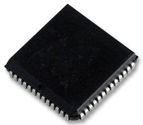
MCU 8-bit 89C 8051 CISC 32KB Flash 3.3V 52-Pin PLCC Stick, AT89C5131A-S3SUL, Microchip

AT89C5131A-L is a high-performance Flash version of the 80C51 single-chip 8-bit microcontrollers with full speed USB functions. AT89C5131A-L features a full-speed USB module compatible with the USB specifications Version 1.1 and 2.0. This module integrates the USB transceivers with a 3.3V voltage regulator and the Serial Interface Engine (SIE) with Digital Phase Locked Loop and 48 MHz clock recovery. USB Event detection logic (Reset and Suspend/Resume) and FIFO buffers supporting the mandatory control Endpoint (EP0) and up to 6 versatile Endpoints with minimum software overhead are also part of the USB module. AT89C5131A-L retains the features of the 80C52 with extended Flash capacity (32-Kbyte), 256 bytes of internal RAM, a 4-level interrupt system, two 16-bit timer/counters (T0/T1), a full duplex enhanced UART (EUART) and an on-chip oscillator.

  • 80C52X2 Core (6 Clocks per Instruction)
    • Maximum Core Frequency 48 MHz in X1 Mode, 24 MHz in X2 Mode
    • Dual Data Pointer
    • Full-duplex Enhanced UART (EUART)
    • Three 16-bit Timer/Counters: T0, T1 and T2
    • 256 Bytes of Scratchpad RAM
  • 16/32-Kbyte On-chip Flash EEPROM In-System Programming through USB
    • Byte and (128 bytes) Erase and Write
    • 100k Write Cycles
  • 3-KbyteFlash EEPROM for Boot loader
    • Byte (128 bytes) Erase and Write
    • 100k Write Cycles
  • 1-Kbyte EEPROM Data
    • Byte and (128 bytes) Erase and Write
    • 100k Write Cycles
  • On-chip Expanded RAM (ERAM): 1024 Bytes
  • Integrated Power Monitor (POR/PFD) to Supervise Internal Power Supply
  • USB 1.1 and 2.0 Full Speed Compliant Module with Interrupt on Transfer Completion
    • Endpoint 0 for Control Transfers: 32-byte FIFO
    • 6 Programmable Endpoints with In or Out Directions and with Bulk, Interrupt or Isochronous Transfers
    • Endpoint 32-byte FIFO
    • Endpoint 2 x 64-byte FIFO with Double Buffering (Ping-pong Mode)
    • Endpoint 6: 2 x 512-byte FIFO with Double Buffering (Ping-pong Mode)
    • Suspend/Resume Interrupts
    • 48 MHz PLL for Full-speed Bus Operation
    • Bus Disconnection on Microcontroller Request
  • 5 Channels Programmable Counter Array (PCA) with 16-bit Counter, High-speed Output, Compare/Capture, PWM and Watchdog Timer Capabilities
  • Programmable Hardware Watchdog Timer (One-time Enabled with Reset-out): 100 ms to 3s at 8 MHz
  • Keyboard Interrupt Interface on Port P1 (8 Bits)
  • TWI (Two Wire Interface) 400Kbit/s
  • SPI Interface (Master/Slave Mode)
  • 34 I/O Pins
  • 4 Direct-drive LED Outputs with Programmable Current Sources: 10 am Typical
  • 4-level Priority Interrupt System (11 sources)
  • Idle and Power-down Modes
  • 0 to 24 MHz On-chip Oscillator with Analog PLL for 48 MHz Synthesis
  • Industrial Temperature Range
  • Extended Range Power Supply: 2.7V to 5.5V (3.3V to 5.5V required for USB)
  • Packages: PLCC52, VQFP64, QFN32.

Характеристики

Бренд

Operating_supply_voltage

3.3 V

Min_operating_supply_voltage

3 V

Max_operating_supply_voltage

3.6 V

Watchdog

1

Supplier_package

PLCC

Specifications

https://4donline.ihs.com/images/VipMasterIC/IC/ATML/ATMLS04537/ATMLS04537-1.pdf?hkey=52A5661711E402568146F3353EA87419

Screening_level

Industrial

Schedule_b

8542310000

Ram_size

1.25 KB

Program_memory_type

Flash

Program_memory_size

32 Kb

Product_dimensions

19.25 x 19.25 x 4.06 mm

Pin_count

52

Operating_temperature

-40 to 85 °C

Number_of_timers

3

Country_of_origin

United States

Number_of_programmable_i_os

34

Msl_level

3

Mounting

Surface Mount

Maximum_speed

48 MHz

Max_processing_temp

245

Lead_finish

Matte Tin

Тип интерфейса

2-Wire/EUART/SPI/USB

Instruction_set_architecture

CISC

Htsn

8542310001

Eccn

3A991.A.2

Device_core

8051

Data_bus_width

8 Bit

Max_expanded_memory_size

64 KB

Артикул: AT89C5131A-S3SUL

Описание

AT89C5131A-L is a high-performance Flash version of the 80C51 single-chip 8-bit microcontrollers with full speed USB functions. AT89C5131A-L features a full-speed USB module compatible with the USB specifications Version 1.1 and 2.0. This module integrates the USB transceivers with a 3.3V voltage regulator and the Serial Interface Engine (SIE) with Digital Phase Locked Loop and 48 MHz clock recovery. USB Event detection logic (Reset and Suspend/Resume) and FIFO buffers supporting the mandatory control Endpoint (EP0) and up to 6 versatile Endpoints with minimum software overhead are also part of the USB module. AT89C5131A-L retains the features of the 80C52 with extended Flash capacity (32-Kbyte), 256 bytes of internal RAM, a 4-level interrupt system, two 16-bit timer/counters (T0/T1), a full duplex enhanced UART (EUART) and an on-chip oscillator.

  • 80C52X2 Core (6 Clocks per Instruction)
    • Maximum Core Frequency 48 MHz in X1 Mode, 24 MHz in X2 Mode
    • Dual Data Pointer
    • Full-duplex Enhanced UART (EUART)
    • Three 16-bit Timer/Counters: T0, T1 and T2
    • 256 Bytes of Scratchpad RAM
  • 16/32-Kbyte On-chip Flash EEPROM In-System Programming through USB
    • Byte and (128 bytes) Erase and Write
    • 100k Write Cycles
  • 3-KbyteFlash EEPROM for Boot loader
    • Byte (128 bytes) Erase and Write
    • 100k Write Cycles
  • 1-Kbyte EEPROM Data
    • Byte and (128 bytes) Erase and Write
    • 100k Write Cycles
  • On-chip Expanded RAM (ERAM): 1024 Bytes
  • Integrated Power Monitor (POR/PFD) to Supervise Internal Power Supply
  • USB 1.1 and 2.0 Full Speed Compliant Module with Interrupt on Transfer Completion
    • Endpoint 0 for Control Transfers: 32-byte FIFO
    • 6 Programmable Endpoints with In or Out Directions and with Bulk, Interrupt or Isochronous Transfers
    • Endpoint 32-byte FIFO
    • Endpoint 2 x 64-byte FIFO with Double Buffering (Ping-pong Mode)
    • Endpoint 6: 2 x 512-byte FIFO with Double Buffering (Ping-pong Mode)
    • Suspend/Resume Interrupts
    • 48 MHz PLL for Full-speed Bus Operation
    • Bus Disconnection on Microcontroller Request
  • 5 Channels Programmable Counter Array (PCA) with 16-bit Counter, High-speed Output, Compare/Capture, PWM and Watchdog Timer Capabilities
  • Programmable Hardware Watchdog Timer (One-time Enabled with Reset-out): 100 ms to 3s at 8 MHz
  • Keyboard Interrupt Interface on Port P1 (8 Bits)
  • TWI (Two Wire Interface) 400Kbit/s
  • SPI Interface (Master/Slave Mode)
  • 34 I/O Pins
  • 4 Direct-drive LED Outputs with Programmable Current Sources: 10 am Typical
  • 4-level Priority Interrupt System (11 sources)
  • Idle and Power-down Modes
  • 0 to 24 MHz On-chip Oscillator with Analog PLL for 48 MHz Synthesis
  • Industrial Temperature Range
  • Extended Range Power Supply: 2.7V to 5.5V (3.3V to 5.5V required for USB)
  • Packages: PLCC52, VQFP64, QFN32.

Детали

Бренд

Operating_supply_voltage

3.3 V

Min_operating_supply_voltage

3 V

Max_operating_supply_voltage

3.6 V

Watchdog

1

Supplier_package

PLCC

Specifications

https://4donline.ihs.com/images/VipMasterIC/IC/ATML/ATMLS04537/ATMLS04537-1.pdf?hkey=52A5661711E402568146F3353EA87419

Screening_level

Industrial

Schedule_b

8542310000

Ram_size

1.25 KB

Program_memory_type

Flash

Program_memory_size

32 Kb

Product_dimensions

19.25 x 19.25 x 4.06 mm

Pin_count

52

Operating_temperature

-40 to 85 °C

Number_of_timers

3

Country_of_origin

United States

Number_of_programmable_i_os

34

Msl_level

3

Mounting

Surface Mount

Maximum_speed

48 MHz

Max_processing_temp

245

Lead_finish

Matte Tin

Тип интерфейса

2-Wire/EUART/SPI/USB

Instruction_set_architecture

CISC

Htsn

8542310001

Eccn

3A991.A.2

Device_core

8051

Data_bus_width

8 Bit

Max_expanded_memory_size

64 KB