Описание
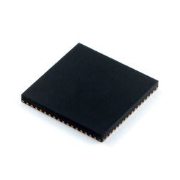
The Microchip AVR XMEGA A3 is a family of low power, high performance and peripheral rich CMOS 8/16-bit microcontrollers based on the AVR enhanced RISC architecture. By executing powerful instructions in a single clock cycle, the XMEGA A3 achieves throughputs approaching 1 Million Instructions Per Second (MIPS) per MHz allowing the system designer to optimize power consumption versus processing speed. The AVR CPU combines a rich instruction set with 32 general purpose working registers. All the 32 registers are directly connected to the Arithmetic Logic Unit (ALU), allowing two independent registers to be accessed in one single instruction, executed in one clock cycle. The resulting architecture is more code efficient while achieving throughputs many times faster than conventional single-accumulator or CISC based microcontrollers. The XMEGA A3 devices provide the following features: In-System Programmable Flash with Read-While-Write capabilities, Internal EEPROM and SRAM, four-channel DMA Controller, eight-channel Event System, Programmable Multi-level Interrupt Controller, 50 general purpose I/O lines, 16-bit Real Time Counter (RTC), seven flexible 16-bit Timer/Counters with compare modes and PWM, seven USARTs, two Two Wire Serial Interfaces (TWIs), three Serial Peripheral Interfaces (SPIs), AES and DES crypto engine, two 8-channel 12-bit ADCs with optional differential input with programmable gain, one 2-channel 12-bit DACs, four analog comparators with window mode, programmable Watchdog Timer with separate Internal Oscillator, accurate internal oscillators with PLL and prescaler and programmable Brown-Out Detection. The Program and Debug Interface (PDI), a fast 2-pin interface for programming and debugging, is available. The devices also have an IEEE std. 1149.1 compliant JTAG test interface, and this can also be used for On-chip Debug and programming.
- High-performance, Low-power 8/16-bit Atmel® AVR® XMEGATM Microcontroller
- Non-volatile Program and Data Memories
- 64 KB – 256 KB of In-System Self-Programmable Flash
- 4 KB – 8 KB Boot Code Section with Independent Lock Bits
- 2 KB – 4 KB EEPROM
- 4 KB – 16 KB Internal SRAM
- Peripheral Features
- Four-channel DMA Controller with support for external requests
- Eight-channel Event System
- Seven 16-bit Timer/Counters
- Four Timer/Counters with 4 Output Compare or Input Capture channels
- Three Timer/Counters with 2 Output Compare or Input Capture channels
- High Resolution Extensions on all Timer/Counters
- Advanced Waveform Extension on one Timer/Counter
- Seven USARTs
- IrDA Extension on 1 USART
- AES and DES Crypto Engine
- Two Two-wire Interfaces with dual address match (I2C and SMBus compatible)
- Three SPI (Serial Peripheral Interfaces)
- 16-bit Real Time Counter with Separate Oscillator
- Two Eight-channel, 12-bit, 2 Msps Analog to Digital Converters
- One Two-channel, 12-bit, 1 Msps Digital to Analog Converter
- Four Analog Comparators with Window compare function
- External Interrupts on all General Purpose I/O pins
- Programmable Watchdog Timer with Separate On-chip Ultra Low Power Oscillator
- Special Microcontroller Features
- Power-on Reset and Programmable Brown-out Detection
- Internal and External Clock Options with PLL
- Programmable Multi-level Interrupt Controller
- Sleep Modes: Idle, Power-down, Standby, Power-save, Extended Standby
- Advanced Programming, Test and Debugging Interfaces
- JTAG (IEEE 1149.1 Compliant) Interface for test, debug and programming
- PDI (Program and Debug Interface) for programming, test and debugging
- I/O and Packages
- 50 Programmable I/O Lines
- 64-lead TQFP
- 64-pad QFN
- Operating Voltage
- 1.6 – 3.6V
- Speed performance
- 0 – 12 MHz @ 1.6 – 3.6V
- 0 – 32 MHz @ 2.7 – 3.6V