Описание
The AVR XMEGA is a family of low power, high performance, and peripheral rich 8-bit microcontrollers based on the AVR enhanced RISC architecture. By executing instructions in a single clock cycle, the AVR XMEGA devices achieve CPU throughput approaching one million instructions per second (MIPS) per megahertz, allowing the system designer to optimize power consumption versus processing speed. The AVR CPU combines a rich instruction set with 32 general purpose working registers. All 32 registers are directly connected to the arithmetic logic unit (ALU), allowing two independent registers to be accessed in a single instruction, executed in one clock cycle. The resulting architecture is more code efficient while achieving throughputs many times faster than conventional single-accumulator or CISC based microcontrollers. The AVR XMEGA A1 devices provide the following features: in-system programmable flash with read-while-write capabilities; internal EEPROM and SRAM; four-channel DMA controller, eight-channel event system and programmable multilevel interrupt controller, 78 general purpose I/O lines, 16-bit real-time counter (RTC); eight flexible, 16-bit timer/counters with compare and PWM channels, eight USARTs; four two-wire serial interfaces (TWIs); four serial peripheral interfaces (SPIs); AES and DES cryptographic engine; two 16-channel, 12-bit ADCs with programmable gain; two 2-channel, 12-bit DACs; four Analog Comparators (ACs) with window mode; programmable watchdog timer with separate internal oscillator; accurate internal oscillators with PLL and presale; and programmable brown-out detection. The program and debug interface (PDI), a fast, two-pin interface for programming and debugging, is available. The devices also have an IEEE std. 1149.1 compliant JTAG interface, and this can also be used for boundary scan, on-chip debug and programming.
- High-performance, low-power AVR® XMEGA® 8-bit Microcontroller
- Nonvolatile program and data memories
- 128KBytes of in-system self-programmable flash
- 4K – 8KBytes boot
- 2 KBBytes EEPROM
- 8 KBBytes internal SRAM
- External bus interface for up to 128Mbit SDRAM
- Special microcontroller features
- Power-on reset and programmable brown-out detection
- Internal and external clock options with PLL and presale
- Programmable multilevel interrupt controller
- Five sleep modes
- Programming and debug interfaces
- JTAG (IEEE 1149.1 compliant) interface, including boundary scan
- PDI (Program and Debug Interface)
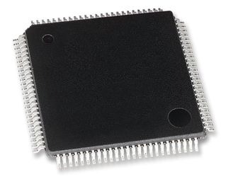
- I/O and packages
- 78 Programmable I/O pins
- 100 lead TQFP
- 100 ball BGA
- 100 ball VFBGA
- Operating voltage
- 1.6 – 3.6V
- Operating frequency
- 0 – 12MHz from 1.6V
- 0 – 32MHz from 2.7V