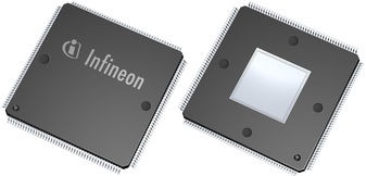
Описание
The TC1762 – member of the Audo-NextGeneration family – is cost optimized for demanding applications where real-time performance and DSP capabilities combined with an outstanding fast interrupt response time and highest level of fault tolerance are required. Audo-NextGeneration is based on the award-winning unified 32-bit TriCore architecture combining RISC, CISC and DSP functionality in a single chip. New groundbreaking peripherals like the Micro Second bus, fast analog-to-digital converter unit or the Micro Link Interface boosting the overall system performance turns the TC1762 into the most cost effective 32-bit microcontroller for high sophisticated applications of the automotive and industrial market.
- High-performance 32-bit super-scaler TriCore v1.3 CPU with 4-stage pipeline
- Superior real-time performance
- Strong bit handling
- Fully integrated DSP capabilities
- Single precision Floating Point Unit (FPU)
- 66 or 80 MHz operation at full temperature range
- Multiple on-chip memories
- 32 Kbyte Local Data Memory (SRAM)
- 4 Kbyte Overlay Memory
- 8 Kbyte Scratch-Pad RAM (SPRAM)
- 8 Kbyte Instruction Cache (ICACHE)
- 1024 Kbyte Flash Memory
- 16 Kbyte Data Flash (2 Kbyte EEPROM emulation)
- 16 Kbyte Boot ROM
- 8-channel DMA Controller
- Fast-response interrupt system with 255 hardware priority arbitration levels serviced by CPU
- High-performance on-chip bus structure
- 64-bit Local Memory Bus (LMB) to Flash memory
- System Peripheral Bus (SPB) for interconnections of functional units
- Versatile on-chip Peripheral Units
- Two Asynchronous/Synchronous Serial Channels (ASCs) with baudrate generator, parity, framing and overrun error detection
- One High Speed Synchronous Serial Channel (SSC) with programmable data length and shift direction
- One Micro Second Bus (MSC) interface for serial port expansion to external power devices
- One high-speed Micro Link Interface (MLI) for serial inter-processor communication
- One MultiCAN Module with two CAN nodes and 64 free assignable message objects for high efficiency data handling via FIFO buffering and gateway data transfer
- One General Purpose Timer Array Module (GPTA) with a powerful set of digital signal filtering and timer functionality to realize autonomous and complex Input/Output management
- One 16-channel Analog-to-Digital Converter unit (ADC) with selectable 8-bit, 10- bit, or 12-bit, supporting 32 input channels
- One 2-channel Fast Analog-to-Digital Converter unit (FADC) with concatenated comb filters for hardware data reduction: supporting 10-bit resolution, with minimum conversion time of 262.5ns (@ 80 MHz) or 318.2ns (@ 66 MHz)
- 32 analog input lines for ADC and FADC
- 81 digital general purpose I/O lines
- Digital I/O ports with 3.3 V capability
- On-chip debug support for OCDS Level 1 and 2 (CPU, DMA)
- Dedicated Emulation Device chip for multi-core debugging, tracing, and calibration via USB V1.1 interface available (TC1766ED)
- Power Management System
- Clock Generation Unit with PLL
- Core supply voltage of 1.5 V
- I/O voltage of 3.3 V
- Full automotive temperature range: -40° to +125°C
- PG-LQFP-176-2 package