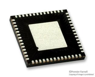
MCU 32-Bit PSoC 4 ARM Cortex M0 RISC 256KB Flash 3.3V/5V 56-Pin QFN, CY8C4128LQI-BL483, Rochester Electronics

PSoC 4 is a scalable and reconfigurable platform architecture for a family of programmable embedded system controllers with an ARM Cortex-M0 CPU. It combines programmable and reconfigurable analog and digital blocks with flexible automatic routing. The PSoC 4128_BLE product family, based on this platform, is a combination of a microcontroller with an integrated Bluetooth Low Energy (BLE), also known as Bluetooth Smart, radio and subsystem (BLESS). The other features include digital programmable logic, high-performance analog-to-digital conversion (ADC), opamps with Comparator mode, and standard communication and timing peripherals. The PSoC 4XX8_BLE products will be fully upward compatible with members of the PSoC 4 platform for new applications and design needs. The programmable analog and digital subsystems allow flexibility and in-field tuning of the design.

  • 32-bit MCU Subsystem
    • 48-MHz ARM Cortex-M0 CPU with single-cycle multiply
    • Up to 256 KB of flash with Read Accelerator
    • Up to 32 KB of SRAM
  • BLE Radio and Subsystem
    • 2.4-GHz RF transceiver with 50-? antenna drive
    • Digital PHY
    • Link-Layer engine supporting master and slave modes
    • RF output power: –18 dBm to +3 dBm
    • RX sensitivity: –92 dBm
    • RX current: 18.7 mA
    • TX current: 16.5 mA at 0 dBm
    • RSSI: 1-dB resolution
  • Programmable Analog
    • Four opamps with reconfigurable high-drive external and high-bandwidth internal drive, Comparator modes, and ADC input buffering capability. Can operate in Deep Sleep mode.
    • 12-bit, 1-Msps SAR ADC with differential and single-ended modes; Channel Sequencer with signal averaging
    • Two current DACs (IDACs) for general-purpose or capacitive sensing applications on any pin
    • Two low-power comparators that operate in Deep Sleep mode
  • Programmable Digital
    • Four programmable logic blocks called universal digital blocks, (UDBs), each with eight macrocells and data path
    • provided peripheral component library, user-defined state machines, and Verilog input
  • Power Management
    • Active mode: 1.7 mA at 3-MHz flash program execution
    • Deep Sleep mode: 1.3 µA with watch crystal oscillator (WCO) on
    • Hibernate mode: 150 nA with RAM retention
    • Stop mode: 60 nA
  • Timing and Pulse-Width Modulation
    • Four 16-bit timer/counter pulse-width modulator (TCPWM) blocks
    • Center-aligned, Edge, and Pseudo-random modes
    • Comparator-based triggering of Kill signals for motor drive and other high-reliability digital logic applications
  • Up to 36 Programmable GPIOs
    • 7 mm × 7 mm 56-pin QFN package
    • 76-ball CSP and thin CSP packages
    • Any GPIO pin can be CapSense, LCD, analog, or digital
    • Two overvoltage-tolerant (OVT) pins; drive modes, strengths, and slew rates are programmable
  • PSoC Creator™ Design Environment
    • Integrated Design Environment (IDE) provides schematic design entry and build (with analog and digital automatic routing)
    • API components for all fixed-function and programmable peripherals
  • Industry-Standard Tool Compatibility
    • After schematic entry, development can be done with ARM-based industry-standard development tools

Характеристики

Program_memory_type

Flash

Supplier_package

QFN

Specifications

https://4donline.ihs.com/images/VipMasterIC/IC/CYPR/CYPR-S-A0005242113/CYPR-S-A0005242113-1.pdf?hkey=52A5661711E402568146F3353EA87419

Special_features

LCD Controller

Screening_level

Industrial

Schedule_b

8542390000

Ram_size

4 KB

Program_memory_size

32 Kb

Product_dimensions

7 x 7 x 0.55 mm

Pin_count

56

Operating_temperature

-40 to 85 °C

Operating_supply_voltage

3.3, 5 V

Watchdog

1

Analog_comparators

2

Eccn

3A991.A.2

Instruction_set_architecture

RISC

Htsn

8542310001

Тип интерфейса

I2C/SPI/UART

Device_core

ARM Cortex M0

Data_bus_width

32 Bit

Country_of_origin

United States

Бренд

Min_operating_supply_voltage

1.71 V

Number_of_timers

4

Number_of_programmable_i_os

36

Msl_level

3

Mounting

Surface Mount

Max_speed

24 MHz

Max_processing_temp

260 °C

Max_operating_supply_voltage

5.5 V

Lead_finish

Gold Over Nickel Palladium

Артикул: CY8C4128LQI-BL483

Описание

PSoC 4 is a scalable and reconfigurable platform architecture for a family of programmable embedded system controllers with an ARM Cortex-M0 CPU. It combines programmable and reconfigurable analog and digital blocks with flexible automatic routing. The PSoC 4128_BLE product family, based on this platform, is a combination of a microcontroller with an integrated Bluetooth Low Energy (BLE), also known as Bluetooth Smart, radio and subsystem (BLESS). The other features include digital programmable logic, high-performance analog-to-digital conversion (ADC), opamps with Comparator mode, and standard communication and timing peripherals. The PSoC 4XX8_BLE products will be fully upward compatible with members of the PSoC 4 platform for new applications and design needs. The programmable analog and digital subsystems allow flexibility and in-field tuning of the design.

  • 32-bit MCU Subsystem
    • 48-MHz ARM Cortex-M0 CPU with single-cycle multiply
    • Up to 256 KB of flash with Read Accelerator
    • Up to 32 KB of SRAM
  • BLE Radio and Subsystem
    • 2.4-GHz RF transceiver with 50-? antenna drive
    • Digital PHY
    • Link-Layer engine supporting master and slave modes
    • RF output power: –18 dBm to +3 dBm
    • RX sensitivity: –92 dBm
    • RX current: 18.7 mA
    • TX current: 16.5 mA at 0 dBm
    • RSSI: 1-dB resolution
  • Programmable Analog
    • Four opamps with reconfigurable high-drive external and high-bandwidth internal drive, Comparator modes, and ADC input buffering capability. Can operate in Deep Sleep mode.
    • 12-bit, 1-Msps SAR ADC with differential and single-ended modes; Channel Sequencer with signal averaging
    • Two current DACs (IDACs) for general-purpose or capacitive sensing applications on any pin
    • Two low-power comparators that operate in Deep Sleep mode
  • Programmable Digital
    • Four programmable logic blocks called universal digital blocks, (UDBs), each with eight macrocells and data path
    • provided peripheral component library, user-defined state machines, and Verilog input
  • Power Management
    • Active mode: 1.7 mA at 3-MHz flash program execution
    • Deep Sleep mode: 1.3 µA with watch crystal oscillator (WCO) on
    • Hibernate mode: 150 nA with RAM retention
    • Stop mode: 60 nA
  • Timing and Pulse-Width Modulation
    • Four 16-bit timer/counter pulse-width modulator (TCPWM) blocks
    • Center-aligned, Edge, and Pseudo-random modes
    • Comparator-based triggering of Kill signals for motor drive and other high-reliability digital logic applications
  • Up to 36 Programmable GPIOs
    • 7 mm × 7 mm 56-pin QFN package
    • 76-ball CSP and thin CSP packages
    • Any GPIO pin can be CapSense, LCD, analog, or digital
    • Two overvoltage-tolerant (OVT) pins; drive modes, strengths, and slew rates are programmable
  • PSoC Creator™ Design Environment
    • Integrated Design Environment (IDE) provides schematic design entry and build (with analog and digital automatic routing)
    • API components for all fixed-function and programmable peripherals
  • Industry-Standard Tool Compatibility
    • After schematic entry, development can be done with ARM-based industry-standard development tools

Детали

Program_memory_type

Flash

Supplier_package

QFN

Specifications

https://4donline.ihs.com/images/VipMasterIC/IC/CYPR/CYPR-S-A0005242113/CYPR-S-A0005242113-1.pdf?hkey=52A5661711E402568146F3353EA87419

Special_features

LCD Controller

Screening_level

Industrial

Schedule_b

8542390000

Ram_size

4 KB

Program_memory_size

32 Kb

Product_dimensions

7 x 7 x 0.55 mm

Pin_count

56

Operating_temperature

-40 to 85 °C

Operating_supply_voltage

3.3, 5 V

Watchdog

1

Analog_comparators

2

Eccn

3A991.A.2

Instruction_set_architecture

RISC

Htsn

8542310001

Тип интерфейса

I2C/SPI/UART

Device_core

ARM Cortex M0

Data_bus_width

32 Bit

Country_of_origin

United States

Бренд

Min_operating_supply_voltage

1.71 V

Number_of_timers

4

Number_of_programmable_i_os

36

Msl_level

3

Mounting

Surface Mount

Max_speed

24 MHz

Max_processing_temp

260 °C

Max_operating_supply_voltage

5.5 V

Lead_finish

Gold Over Nickel Palladium