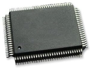
MCU 32-Bit Piccolo F2806x C28x RISC 128KB Flash 1.8V/3.3V 100-Pin LQFP, TMS320F28069PZA, Texas Instruments

  The F2806x Piccolo family of microcontrollers (MCUs) provides the power of the C28x core and CLA coupled with highly integrated control peripherals in low pin-count devices. This family is code-compatible with previous C28x-based code, and also provides a high level of analog integration. An internal voltage regulator allows for single-rail operation. Enhancements have been made to the High-Resolution Pulse Width Modulator (HRPWM) module to allow for dual-edge control (frequency modulation). Analog comparators with internal 10-bit references have been added and can be routed directly to control the ePWM outputs. The ADC converts from 0 to 3.3-V fixed full-scale range and supports ratio-metric VREFHI/VREFLO references. The ADC interface has been optimized for low overhead and latency. 

  • High-Efficiency 32-Bit CPU (TMS320C28x)
    • 90 MHz (11.11-ns Cycle Time)
    • 16 x 16 and 32 x 32 Multiply and Accumulate (MAC) Operations
    • 16 x 16 Dual MAC
    • Harvard Bus Architecture
    • Atomic Operations
    • Fast Interrupt Response and Processing
    • Unified Memory Programming Model
    • Code-Efficient (in C/C++ and Assembly)
  • Floating-Point Unit(FPU)
    • Native Single-Precision Floating-Point Operations
  • Programmable Control Law Accelerator(CLA)
    • 32-Bit Floating-Point Math Accelerator
    • Executes Code Independently of the Main CPU
  • Viterbi, ComplexMath, CRC Unit (VCU)
    • Extends C28x Instruction Set to Support Complex Multiply, Viterbi Operations, and Cyclic Redundency Check (CRC)
  • Embedded Memory
    • Up to 256KB of Flash
    • Up to 100KB of RAM
    • 2KB of One-Time Programmable (OTP) ROM
  • 6-Channel Direct Memory Access(DMA)
  • Low Device and System Cost
    • Single 3.3-V Supply
    • No Power Sequencing Requirement
    • Integrated Power-on Reset and Brown-out Reset
    • Low-Power Operating Modes
    • No Analog Support Pin
  • Endianness: LittleEndian
  • JTAG Boundary Scan Support
    • IEEE Standard 1149.1-1990 Standard Test Access Port and Boundary Scan Architecture
  • Clocking
    • Two Internal Zero-Pin Oscillators
    • On-Chip Crystal Oscillator/External Clock Input
    • Watchdog Timer Module
    • Missing Clock Detection Circuitry
  • Peripheral Interrupt Expansion (PIE) BlockThat Supports All Peripheral Interrupts
  • Three 32-Bit CPUTimers
  • Advanced Control Peripherals
  • Up to 8 EnhancedPulse-Width Modulator (ePWM) Modules
    • 16 PWM Channels Total (8 HRPWM-Capable)
    • Independent 16-Bit Timer in Each Module
  • Three Input Enhanced Capture (eCAP)Modules
  • Up to 4 High-Resolution Capture (HRCAP) Modules
  • Upto 2 Enhanced Quadrature Encoder Pulse (eQEP) Modules
  • 12-Bit Analog-to-DigitalConverter (ADC), Dual Sample-and-Hold (S/H)
    • Up to 3.46 MSPS
    • Up to 16 Channels
  • On-Chip TemperatureSensor
  • 128-Bit Security Key and Lock
    • Protects Secure Memory Blocks
    • Prevents Reverse-Engineering of Firmware
  • Serial PortPeripherals
    • Two Serial Communications Interface (SCI) [UART] Modules
    • Two Serial Peripheral Interface (SPI) Modules
    • One Inter-Integrated-Circuit (I2C) Bus
    • One Multichannel Buffered Serial Port (McBSP) Bus
    • One Enhanced Controller Area Network (eCAN)
    • Universal Serial Bus (USB) 2.0
      (see Device Comparison Table for Availability)
      • Full-Speed Device Mode
      • Full-Speed or Low-Speed Host Mode
  • Up to54 Individually Programmable, Multiplexed General-Purpose Input/Output (GPIO) Pins With InputFiltering
  • Advanced Emulation Features
    • Analysis and Breakpoint Functions
    • Real-Time Debug via Hardware
  • 2806x Packages
    • 80-Pin PFP and 100-Pin PZP PowerPAD Thermally Enhanced Thin Quad Flatpacks (HTQFPs)
    • 80-Pin PN and 100-Pin PZ Low-Profile Quad Flatpacks (LQFPs)
  • Характеристики

    Analog_comparators

    3

    Specifications

    http://www.ti.com/general/docs/lit/getliterature.tsp?genericPartNumber=TMS320F28067&&fileType=pdf

    Number_of_programmable_i_os

    54

    Number_of_timers

    3

    On_chip_adc

    16-chx12-bit

    Operating_supply_voltage

    1.8, 3.3 V

    Operating_temperature

    -40 to 85 °C

    Pin_count

    100

    Product_dimensions

    14 x 14 x 1.4

    Program_memory_type

    Flash

    Mounting

    Surface Mount

    Ram_size

    256 KB

    Schedule_b

    8542310000

    Screening_level

    Industrial

    Special_features

    CAN Controller

    Program_memory_size

    128 KB

    Watchdog

    1

    Supplier_package

    LQFP

    Msl_level

    3

    Min_operating_supply_voltage

    1.71, 2.97 V

    Бренд

    Country_of_origin

    United States

    Data_bus_width

    32 Bit

    Device_core

    C28x

    Eccn

    3A991.A.2

    Htsn

    8542310001

    Max_speed

    90 MHz

    Instruction_set_architecture

    RISC

    Тип интерфейса

    CAN/I2C/SCI/SPI/UART

    Lead_finish

    Gold Over Nickel Palladium

    Max_operating_supply_voltage

    1.995, 3.63 V

    Max_processing_temp

    260 °C

    Артикул: TMS320F28069PZA

    Описание

      The F2806x Piccolo family of microcontrollers (MCUs) provides the power of the C28x core and CLA coupled with highly integrated control peripherals in low pin-count devices. This family is code-compatible with previous C28x-based code, and also provides a high level of analog integration. An internal voltage regulator allows for single-rail operation. Enhancements have been made to the High-Resolution Pulse Width Modulator (HRPWM) module to allow for dual-edge control (frequency modulation). Analog comparators with internal 10-bit references have been added and can be routed directly to control the ePWM outputs. The ADC converts from 0 to 3.3-V fixed full-scale range and supports ratio-metric VREFHI/VREFLO references. The ADC interface has been optimized for low overhead and latency. 

  • High-Efficiency 32-Bit CPU (TMS320C28x)
    • 90 MHz (11.11-ns Cycle Time)
    • 16 x 16 and 32 x 32 Multiply and Accumulate (MAC) Operations
    • 16 x 16 Dual MAC
    • Harvard Bus Architecture
    • Atomic Operations
    • Fast Interrupt Response and Processing
    • Unified Memory Programming Model
    • Code-Efficient (in C/C++ and Assembly)
  • Floating-Point Unit(FPU)
    • Native Single-Precision Floating-Point Operations
  • Programmable Control Law Accelerator(CLA)
    • 32-Bit Floating-Point Math Accelerator
    • Executes Code Independently of the Main CPU
  • Viterbi, ComplexMath, CRC Unit (VCU)
    • Extends C28x Instruction Set to Support Complex Multiply, Viterbi Operations, and Cyclic Redundency Check (CRC)
  • Embedded Memory
    • Up to 256KB of Flash
    • Up to 100KB of RAM
    • 2KB of One-Time Programmable (OTP) ROM
  • 6-Channel Direct Memory Access(DMA)
  • Low Device and System Cost
    • Single 3.3-V Supply
    • No Power Sequencing Requirement
    • Integrated Power-on Reset and Brown-out Reset
    • Low-Power Operating Modes
    • No Analog Support Pin
  • Endianness: LittleEndian
  • JTAG Boundary Scan Support
    • IEEE Standard 1149.1-1990 Standard Test Access Port and Boundary Scan Architecture
  • Clocking
    • Two Internal Zero-Pin Oscillators
    • On-Chip Crystal Oscillator/External Clock Input
    • Watchdog Timer Module
    • Missing Clock Detection Circuitry
  • Peripheral Interrupt Expansion (PIE) BlockThat Supports All Peripheral Interrupts
  • Three 32-Bit CPUTimers
  • Advanced Control Peripherals
  • Up to 8 EnhancedPulse-Width Modulator (ePWM) Modules
    • 16 PWM Channels Total (8 HRPWM-Capable)
    • Independent 16-Bit Timer in Each Module
  • Three Input Enhanced Capture (eCAP)Modules
  • Up to 4 High-Resolution Capture (HRCAP) Modules
  • Upto 2 Enhanced Quadrature Encoder Pulse (eQEP) Modules
  • 12-Bit Analog-to-DigitalConverter (ADC), Dual Sample-and-Hold (S/H)
    • Up to 3.46 MSPS
    • Up to 16 Channels
  • On-Chip TemperatureSensor
  • 128-Bit Security Key and Lock
    • Protects Secure Memory Blocks
    • Prevents Reverse-Engineering of Firmware
  • Serial PortPeripherals
    • Two Serial Communications Interface (SCI) [UART] Modules
    • Two Serial Peripheral Interface (SPI) Modules
    • One Inter-Integrated-Circuit (I2C) Bus
    • One Multichannel Buffered Serial Port (McBSP) Bus
    • One Enhanced Controller Area Network (eCAN)
    • Universal Serial Bus (USB) 2.0
      (see Device Comparison Table for Availability)
      • Full-Speed Device Mode
      • Full-Speed or Low-Speed Host Mode
  • Up to54 Individually Programmable, Multiplexed General-Purpose Input/Output (GPIO) Pins With InputFiltering
  • Advanced Emulation Features
    • Analysis and Breakpoint Functions
    • Real-Time Debug via Hardware
  • 2806x Packages
    • 80-Pin PFP and 100-Pin PZP PowerPAD Thermally Enhanced Thin Quad Flatpacks (HTQFPs)
    • 80-Pin PN and 100-Pin PZ Low-Profile Quad Flatpacks (LQFPs)
  • Детали

    Analog_comparators

    3

    Specifications

    http://www.ti.com/general/docs/lit/getliterature.tsp?genericPartNumber=TMS320F28067&&fileType=pdf

    Number_of_programmable_i_os

    54

    Number_of_timers

    3

    On_chip_adc

    16-chx12-bit

    Operating_supply_voltage

    1.8, 3.3 V

    Operating_temperature

    -40 to 85 °C

    Pin_count

    100

    Product_dimensions

    14 x 14 x 1.4

    Program_memory_type

    Flash

    Mounting

    Surface Mount

    Ram_size

    256 KB

    Schedule_b

    8542310000

    Screening_level

    Industrial

    Special_features

    CAN Controller

    Program_memory_size

    128 KB

    Watchdog

    1

    Supplier_package

    LQFP

    Msl_level

    3

    Min_operating_supply_voltage

    1.71, 2.97 V

    Бренд

    Country_of_origin

    United States

    Data_bus_width

    32 Bit

    Device_core

    C28x

    Eccn

    3A991.A.2

    Htsn

    8542310001

    Max_speed

    90 MHz

    Instruction_set_architecture

    RISC

    Тип интерфейса

    CAN/I2C/SCI/SPI/UART

    Lead_finish

    Gold Over Nickel Palladium

    Max_operating_supply_voltage

    1.995, 3.63 V

    Max_processing_temp

    260 °C