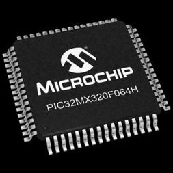
MCU 32-bit PIC32 PIC RISC 64KB Flash 2.5V/3.3V 64-Pin QFN EP Tube, PIC32MX320F064H-80V/MR, Microchip

PIC32MX320F064H High-Performance, General Purpose and USB, 32-bit Flash Microcontrollers The MIPS32 M4K Processor Core is the heart of the PIC32MX3XX/4XX family processor. The CPU fetches instructions, decodes each instruction, fetches source operands, executes each inst ruction and writes the results of instruction execut ion to the proper destinations The MIPS32 M4K Processor Core contains several logic blocks working together in parallel, providing an efficient high performance computing engine. The following blocks are included with the core: Execution Unit Multiply/Divide Unit (MDU) System Control Coprocessor (CP0) Fixed Mapping Translation (FMT) Dual Internal Bus interfaces Power Management MIPS16e Support Enhanced JTAG (EJTAG) Controller The MIPS32 M4K Processor Core execution unit implements a load/store architecture with single-cycle ALU operations (logical, shift, add, subtract) and an autonomous multiply/divide unit. The core contains thirty-two 32-bit general purpose registers used for integer operations and address calculation. One addi- tional register file shadow set (containing thirty-two registers) is added to minimize context switching overhead during interrupt/exception processing. The register file consists of two read ports and one write port and is fully bypassed to minimize operation latency in the pipeline. The execution unit includes: 32-bit adder used for calculating the data address Address unit for calculating the next instruction address Logic for branch determination and branch target address calculation Load aligner Bypass multiplexers used to avoid stalls when executing instructions streams where data producing instructions are followed closely by consumers of their results Leading Zero/One detect unit for implementing the CLZ and CLO instructions Arithmetic Logic Unit (A LU) for performing bitwise logical operations Shifter and Store Aligner The MIPS32 M4K Processor Core includes a multiply/divide unit (MDU) that contains a separate pipeline for multiply and divide operations. This pipeline oper- ates in parallel with the integer unit (IU) pipeline and does not stall when the IU pipeline stalls. This allows MDU operations to be part ially masked by system stalls and/or other integer unit instructions The high-performance MDU consists of a 32×16 booth recoded multiplier, result/accumulation registers (HI and LO), a divide state machine, and the necessary multiplexers and control logic. The first number shown (‘32’ of 32×16) represents the rs operand. The second number (‘16’ of 32×16) represents the rt operand. The PIC32MX core only checks the value of the latter (rt) operand to determine how many times the operation must pass through the multiplier. The 16×16 and 32×16 operations pass through the multiplier once. A 32×32 operation passes through the multiplier twice The MDU supports execution of one 16×16 or 32×16 multiply operation every clock cycle; 32×32 multiply operations can be issued every other clock cycle. Appropriate interlocks are implemented to stall the issuance of back-to-back 32×32 multiply operations. The multiply operand size is automatically determined by logic built into the MDU Divide operations are impl emented with a simple 1 bit per clock iterative algorithm. An early-in detection checks the sign extensio n of the dividend (rs) operand. If rs is 8 bits wide, 23 iterations are skipped. For a 16- bit-wide rs, 15 iterations are skipped, and for a 24-bit- wide rs, 7 iterations are skipped. Any attempt to issue a subsequent MDU instruction while a divide is still active causes an IU pipeline stall until the divide operation is completed

  • High-Performance 32-bit RISC CPU:
  • MIPS32® M4K® 32-bit core with 5-stage pipeline
  • 80 MHz maximum frequency
  • 1.56 DMIPS/MHz (Dhrystone 2.1) performance at 0 wait state Flash access
  • Single-cycle multiply and high-performance divide unit
  • MIPS16e® mode for up to 40% smaller code size
  • Two sets of 32 core register files (32-bit) to reduce interrupt latency
  • Prefetch Cache module to speed execution from Flash
  • Microcontroller Features:
  • Operating temperature range of -40°C to +105°C
  • Operating voltage range of 2.3V to 3.6V
  • 32K to 512K Flash memory (plus an additional 12 KB of boot Flash)
  • 8K to 32K SRAM memory
  • Pin-compatible with most PIC24/dsPIC® DSC devices
  • Multiple power management modes
  • Multiple interrupt vectors with individually programmable priority
  • Fail-Safe Clock Monitor Mode
  • Configurable Watchdog Timer with on-chip Low-Power RC Oscillator for reliable operation
  • Peripheral Features:
  • Atomic SET, CLEAR and INVERT operation on select peripheral registers
  • Up to 4-channel hardware DMA with automatic data size detection
  • USB 2.0-compliant full-speed device and
  • On-The-Go (OTG) controller
  • USB has a dedicated DMA channel
  • 3 MHz to 25 MHz crystal oscillator
  • Internal 8 MHz and 32 kHz oscillators
  • Separate PLLs for CPU and USB clocks
  • Two I2C™ modules
  • Two UART modules with:
    • RS-232, RS-485 and LIN support -IrDA® with on-chip hardware encoder and decoder
  • Up to two SPI modules
  • Parallel Master and Slave Port (PMP/PSP) with 8-bit and 16-bit data and up to 16 address lines
  • Hardware Real-Time Clock and Calendar (RTCC)
  • Five 16-bit Timers/Counters (two 16-bit pairs combine to create two 32-bit timers)
  • Five capture inputs
  • Five compare/PWM outputs
  • Five external interrupt pins
  • High-Speed I/O pins capable of toggling at up to 80 MHz
  • High-current sink/source (18 mA/18 mA) on all I/O pins
  • Configurable open-drain output on digital I/O pins Debug Features:
  • Two programming and debugging Interfaces:
    • 2-wire interface with unintrusive access and real-time data exchange with application
    • 4-wire MIPS® standard enhanced JTAG interface
  • Unintrusive hardware-based instruction trace
  • IEEE Standard 1149.2-compatible (JTAG) boundary scan Analog Features:
  • Up to 16-channel 10-bit Analog-to-Digital Converter:
    • 1000 ksps conversion rate
    • Conversion available during Sleep, Idle
  • Two Analog Comparators

Характеристики

Analog_comparators

2

Watchdog

1

Number_of_programmable_i_os

53

Number_of_timers

5

On_chip_adc

16-chx10-bit

Operating_supply_voltage

2.5, 3.3 V

Operating_temperature

-40 to 105 °C

Pin_count

64

Product_dimensions

9 x 9 x 0.88 mm

Program_memory_type

Flash

Mounting

Surface Mount

Ram_size

16 Kb

Schedule_b

8542310000

Specifications

https://4donline.ihs.com/images/VipMasterIC/IC/MCHP/MCHPS03432/MCHPS03432-1.pdf?hkey=52A5661711E402568146F3353EA87419

Supplier_package

QFN EP

Program_memory_size

64 KB

Min_operating_supply_voltage

2.3 V

Msl_level

1

Бренд

Country_of_origin

China

Data_bus_width

32 Bit

Data_memory_size

16 KB

Device_core

PIC

Eccn

3A991.A.2

Htsn

8542310001

Max_speed

80 MHz

Instruction_set_architecture

RISC

Тип интерфейса

I2C/SPI/UART

Lead_finish

Matte Tin

Max_expanded_memory_size

4 GB

Max_operating_supply_voltage

3.6 V

Max_processing_temp

260 °C

Артикул: PIC32MX320F064H-80V/MR

Описание

PIC32MX320F064H High-Performance, General Purpose and USB, 32-bit Flash Microcontrollers The MIPS32 M4K Processor Core is the heart of the PIC32MX3XX/4XX family processor. The CPU fetches instructions, decodes each instruction, fetches source operands, executes each inst ruction and writes the results of instruction execut ion to the proper destinations The MIPS32 M4K Processor Core contains several logic blocks working together in parallel, providing an efficient high performance computing engine. The following blocks are included with the core: Execution Unit Multiply/Divide Unit (MDU) System Control Coprocessor (CP0) Fixed Mapping Translation (FMT) Dual Internal Bus interfaces Power Management MIPS16e Support Enhanced JTAG (EJTAG) Controller The MIPS32 M4K Processor Core execution unit implements a load/store architecture with single-cycle ALU operations (logical, shift, add, subtract) and an autonomous multiply/divide unit. The core contains thirty-two 32-bit general purpose registers used for integer operations and address calculation. One addi- tional register file shadow set (containing thirty-two registers) is added to minimize context switching overhead during interrupt/exception processing. The register file consists of two read ports and one write port and is fully bypassed to minimize operation latency in the pipeline. The execution unit includes: 32-bit adder used for calculating the data address Address unit for calculating the next instruction address Logic for branch determination and branch target address calculation Load aligner Bypass multiplexers used to avoid stalls when executing instructions streams where data producing instructions are followed closely by consumers of their results Leading Zero/One detect unit for implementing the CLZ and CLO instructions Arithmetic Logic Unit (A LU) for performing bitwise logical operations Shifter and Store Aligner The MIPS32 M4K Processor Core includes a multiply/divide unit (MDU) that contains a separate pipeline for multiply and divide operations. This pipeline oper- ates in parallel with the integer unit (IU) pipeline and does not stall when the IU pipeline stalls. This allows MDU operations to be part ially masked by system stalls and/or other integer unit instructions The high-performance MDU consists of a 32×16 booth recoded multiplier, result/accumulation registers (HI and LO), a divide state machine, and the necessary multiplexers and control logic. The first number shown (‘32’ of 32×16) represents the rs operand. The second number (‘16’ of 32×16) represents the rt operand. The PIC32MX core only checks the value of the latter (rt) operand to determine how many times the operation must pass through the multiplier. The 16×16 and 32×16 operations pass through the multiplier once. A 32×32 operation passes through the multiplier twice The MDU supports execution of one 16×16 or 32×16 multiply operation every clock cycle; 32×32 multiply operations can be issued every other clock cycle. Appropriate interlocks are implemented to stall the issuance of back-to-back 32×32 multiply operations. The multiply operand size is automatically determined by logic built into the MDU Divide operations are impl emented with a simple 1 bit per clock iterative algorithm. An early-in detection checks the sign extensio n of the dividend (rs) operand. If rs is 8 bits wide, 23 iterations are skipped. For a 16- bit-wide rs, 15 iterations are skipped, and for a 24-bit- wide rs, 7 iterations are skipped. Any attempt to issue a subsequent MDU instruction while a divide is still active causes an IU pipeline stall until the divide operation is completed

  • High-Performance 32-bit RISC CPU:
  • MIPS32® M4K® 32-bit core with 5-stage pipeline
  • 80 MHz maximum frequency
  • 1.56 DMIPS/MHz (Dhrystone 2.1) performance at 0 wait state Flash access
  • Single-cycle multiply and high-performance divide unit
  • MIPS16e® mode for up to 40% smaller code size
  • Two sets of 32 core register files (32-bit) to reduce interrupt latency
  • Prefetch Cache module to speed execution from Flash
  • Microcontroller Features:
  • Operating temperature range of -40°C to +105°C
  • Operating voltage range of 2.3V to 3.6V
  • 32K to 512K Flash memory (plus an additional 12 KB of boot Flash)
  • 8K to 32K SRAM memory
  • Pin-compatible with most PIC24/dsPIC® DSC devices
  • Multiple power management modes
  • Multiple interrupt vectors with individually programmable priority
  • Fail-Safe Clock Monitor Mode
  • Configurable Watchdog Timer with on-chip Low-Power RC Oscillator for reliable operation
  • Peripheral Features:
  • Atomic SET, CLEAR and INVERT operation on select peripheral registers
  • Up to 4-channel hardware DMA with automatic data size detection
  • USB 2.0-compliant full-speed device and
  • On-The-Go (OTG) controller
  • USB has a dedicated DMA channel
  • 3 MHz to 25 MHz crystal oscillator
  • Internal 8 MHz and 32 kHz oscillators
  • Separate PLLs for CPU and USB clocks
  • Two I2C™ modules
  • Two UART modules with:
    • RS-232, RS-485 and LIN support -IrDA® with on-chip hardware encoder and decoder
  • Up to two SPI modules
  • Parallel Master and Slave Port (PMP/PSP) with 8-bit and 16-bit data and up to 16 address lines
  • Hardware Real-Time Clock and Calendar (RTCC)
  • Five 16-bit Timers/Counters (two 16-bit pairs combine to create two 32-bit timers)
  • Five capture inputs
  • Five compare/PWM outputs
  • Five external interrupt pins
  • High-Speed I/O pins capable of toggling at up to 80 MHz
  • High-current sink/source (18 mA/18 mA) on all I/O pins
  • Configurable open-drain output on digital I/O pins Debug Features:
  • Two programming and debugging Interfaces:
    • 2-wire interface with unintrusive access and real-time data exchange with application
    • 4-wire MIPS® standard enhanced JTAG interface
  • Unintrusive hardware-based instruction trace
  • IEEE Standard 1149.2-compatible (JTAG) boundary scan Analog Features:
  • Up to 16-channel 10-bit Analog-to-Digital Converter:
    • 1000 ksps conversion rate
    • Conversion available during Sleep, Idle
  • Two Analog Comparators

Детали

Analog_comparators

2

Watchdog

1

Number_of_programmable_i_os

53

Number_of_timers

5

On_chip_adc

16-chx10-bit

Operating_supply_voltage

2.5, 3.3 V

Operating_temperature

-40 to 105 °C

Pin_count

64

Product_dimensions

9 x 9 x 0.88 mm

Program_memory_type

Flash

Mounting

Surface Mount

Ram_size

16 Kb

Schedule_b

8542310000

Specifications

https://4donline.ihs.com/images/VipMasterIC/IC/MCHP/MCHPS03432/MCHPS03432-1.pdf?hkey=52A5661711E402568146F3353EA87419

Supplier_package

QFN EP

Program_memory_size

64 KB

Min_operating_supply_voltage

2.3 V

Msl_level

1

Бренд

Country_of_origin

China

Data_bus_width

32 Bit

Data_memory_size

16 KB

Device_core

PIC

Eccn

3A991.A.2

Htsn

8542310001

Max_speed

80 MHz

Instruction_set_architecture

RISC

Тип интерфейса

I2C/SPI/UART

Lead_finish

Matte Tin

Max_expanded_memory_size

4 GB

Max_operating_supply_voltage

3.6 V

Max_processing_temp

260 °C