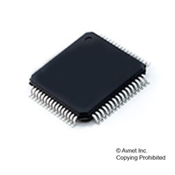
MCU 32-Bit MB9B560L ARM Cortex M4F RISC 288KB Flash 3.3V/5V 64-Pin LQFP, MB9BF564LPMC-G-JNE2, Rochester Electronics

The MB9B564L Series are a highly integrated 32-bit microcontrollers dedicated for embedded controllers with high-performance and competitive cost. These series are based on the ARM Cortex-M4F Processor with on-chip Flash memory and SRAM, and has peripheral functions such as Motor Control Timers, ADCs and Communication Interfaces (USB, CAN, UART, CSIO, I2C, LIN).

  • 32-bit ARM Cortex-M4F Core
    • Processor version: r0p1
    • Up to 160 MHz Frequency Operation
    • FPU built-in
    • Support DSP instruction
    • Memory Protection Unit (MPU): improves the reliability of an embedded system
    • Integrated Nested Vectored Interrupt Controller (NVIC): 1 NMI (non-maskable interrupt) and 128 peripheral interrupts and 16 priority levels
    • 24-bit System timer (Sys Tick): System timer for OS task management
  • On-chip Memories [Flash memory] These series are based on two independent on-chip Flash memories.
    • MainFlash memory
    • Up to 512 Kbytes
    • Built-in Flash Accelerator System with 16 Kbytes trace buffer memory
    • The read access to Flash memory can be achieved without wait-cycle up to operation frequency of 72 MHz. Even at the operation frequency more than 72 MHz, an equivalent access to Flash memory can be obtained by Flash Accelerator System.
    • Security function for code protection
    • WorkFlash memory
    • 32 Kbytes
    • Read cycle:
    • 6wait-cycle: the operation frequency more than 120 MHz, and up to 160 MHz
    • 4wait-cycle: the operation frequency more than 72 MHz, and up to 120 MHz
    • 2wait-cycle: the operation frequency more than 40 MHz, and up to 72 MHz
    • 0wait-cycle: the operation frequency up to 40MHz
    • Security function is shared with code protection [SRAM] This is composed of three independent SRAMs (SRAM0, SRAM1 and SRAM2). SRAM0 is connected to I-code bus or D-code bus of Cortex-M4F core. SRAM1 and SRAM2 are connected to System bus of Cortex-M4F core.
    • SRAM0: Up to 32 Kbytes
    • SRAM1: Up to 16 Kbytes
    • SRAM2: Up to 16 Kbytes

Характеристики

Program_memory_type

Flash

Supplier_package

LQFP

Specifications

http://www.spansion.com/fjdocuments/fj/datasheet/e-ds/MB9B560L_DS709-00005.pdf

Special_features

CAN Controller

Screening_level

Extended Industrial

Schedule_b

8542390000

Ram_size

64 KB

Program_memory_size

288 KB

Product_dimensions

12 x 12 x 1.4

Pin_count

64

Operating_temperature

-40 to 125 °C

Operating_supply_voltage

3.3, 5 V

Watchdog

2

On_chip_dac

2-chx12-bit

Eccn

EAR99

Instruction_set_architecture

RISC

Htsn

8542390001

Тип интерфейса

CAN/CSIO/I2C/LIN/UART/USB

Device_core

ARM Cortex M4F

Data_bus_width

32 Bit

Country_of_origin

United States

Бренд

On_chip_adc

2(15-chx12-bit)

Min_operating_supply_voltage

2.7 V

Number_of_timers

4

Number_of_programmable_i_os

48

Mounting

Surface Mount

Max_speed

160 MHz

Max_operating_supply_voltage

5.5 V

Артикул: MB9BF564LPMC-G-JNE2

Описание

The MB9B564L Series are a highly integrated 32-bit microcontrollers dedicated for embedded controllers with high-performance and competitive cost. These series are based on the ARM Cortex-M4F Processor with on-chip Flash memory and SRAM, and has peripheral functions such as Motor Control Timers, ADCs and Communication Interfaces (USB, CAN, UART, CSIO, I2C, LIN).

  • 32-bit ARM Cortex-M4F Core
    • Processor version: r0p1
    • Up to 160 MHz Frequency Operation
    • FPU built-in
    • Support DSP instruction
    • Memory Protection Unit (MPU): improves the reliability of an embedded system
    • Integrated Nested Vectored Interrupt Controller (NVIC): 1 NMI (non-maskable interrupt) and 128 peripheral interrupts and 16 priority levels
    • 24-bit System timer (Sys Tick): System timer for OS task management
  • On-chip Memories [Flash memory] These series are based on two independent on-chip Flash memories.
    • MainFlash memory
    • Up to 512 Kbytes
    • Built-in Flash Accelerator System with 16 Kbytes trace buffer memory
    • The read access to Flash memory can be achieved without wait-cycle up to operation frequency of 72 MHz. Even at the operation frequency more than 72 MHz, an equivalent access to Flash memory can be obtained by Flash Accelerator System.
    • Security function for code protection
    • WorkFlash memory
    • 32 Kbytes
    • Read cycle:
    • 6wait-cycle: the operation frequency more than 120 MHz, and up to 160 MHz
    • 4wait-cycle: the operation frequency more than 72 MHz, and up to 120 MHz
    • 2wait-cycle: the operation frequency more than 40 MHz, and up to 72 MHz
    • 0wait-cycle: the operation frequency up to 40MHz
    • Security function is shared with code protection [SRAM] This is composed of three independent SRAMs (SRAM0, SRAM1 and SRAM2). SRAM0 is connected to I-code bus or D-code bus of Cortex-M4F core. SRAM1 and SRAM2 are connected to System bus of Cortex-M4F core.
    • SRAM0: Up to 32 Kbytes
    • SRAM1: Up to 16 Kbytes
    • SRAM2: Up to 16 Kbytes

Детали

Program_memory_type

Flash

Supplier_package

LQFP

Specifications

http://www.spansion.com/fjdocuments/fj/datasheet/e-ds/MB9B560L_DS709-00005.pdf

Special_features

CAN Controller

Screening_level

Extended Industrial

Schedule_b

8542390000

Ram_size

64 KB

Program_memory_size

288 KB

Product_dimensions

12 x 12 x 1.4

Pin_count

64

Operating_temperature

-40 to 125 °C

Operating_supply_voltage

3.3, 5 V

Watchdog

2

On_chip_dac

2-chx12-bit

Eccn

EAR99

Instruction_set_architecture

RISC

Htsn

8542390001

Тип интерфейса

CAN/CSIO/I2C/LIN/UART/USB

Device_core

ARM Cortex M4F

Data_bus_width

32 Bit

Country_of_origin

United States

Бренд

On_chip_adc

2(15-chx12-bit)

Min_operating_supply_voltage

2.7 V

Number_of_timers

4

Number_of_programmable_i_os

48

Mounting

Surface Mount

Max_speed

160 MHz

Max_operating_supply_voltage

5.5 V