Описание
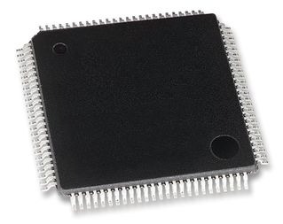
The MB9BF404NA is a highly integrated 32-bit microcontroller that target for high-performance and cost-sensitive embedded control applications. The MB9BF404NA is based on the ARM Cortex-M3 Processor and on-chip Flash memory and SRAM, and peripheral functions, including Motor Control Timers, ADCs and Communication Interfaces (CAN, UART,CSIO, I2C, LIN).
- 32-bit ARM Cortex-M3 Core
- Processor version: r2p0
- Up to 80MHz Frequency Operation
- Memory Protection Unit (MPU): improve the reliability of an embedded system
- Integrated Nested Vectored Interrupt Controller (NVIC): 1 NMI (non-maskable interrupt) and 48 peripheral interrupts and 16 priority levels
- 24-bit System timer (Sys Tick): System timer for OS task management
- On-chip Memories [Flash memory]
- Up to 512 Kbyte
- Read cycle: 0wait-cycle@up to 60MHz, 2wait-cycle above : Instruction pre-fetch buffer is included. So when CPU access continuously, it becomes 0wait-cycle
- Security function for code protection [SRAM] This series contain a total of up to 64Kbyte on-chip SRAM. This is composed of two independent SRAM(SRAM0, SRAM1). SRAM0 is connected to I-code bus and D-code bus of Cortex-M3 core. SRAM1 is connected to System bus.
- SRAM0: Up to 32 Kbyte
- SRAM1: Up to 32 Kbyte
- CAN Interface (Max. 2channels)
- Compatible with CAN Specification 2.0A/B
- Maximum transfer rate: 1 Mbps
- Built-in 32 message buffer
- Multi-function Serial Interface (Max. 8channels)
- 4 channels with 16steps × 9bit FIFO (ch.4-ch.7), 4 channels without FIFO (ch.0-ch.3)
- Operation mode is selectable from the followings for each channel.
- UART
- CSIO
- LIN
- I 2C [UART]
- Full-duplex double buffer
- Selection with or without parity supported
- Built-in dedicated baud rate generator
- External clock available as a serial clock
- Hardware Flow control : Automatically control the transmission by CTS/RTS (only ch.4)
- Various error detect functions available (parity errors, framing errors, and overrun errors) [CSIO]
- Full-duplex double buffer
- Built-in dedicated baud rate generator
- Overrun error detect function available [LIN]
- LIN protocol Rev.2.1 supported
- Full-duplex double buffer
- Master/Slave mode supported
- LIN break field generate (can be changed 13-16bit length)
- LIN break delimiter generate (can be changed 1-4bit length)
- Various error detect functions available (parity errors, framing errors, and overrun errors) [I2C]
- Standard-mode (Max.100kbps) / Fast-mode (Max.400Kbps) supported
- External Bus Interface
- Supports SRAM, NOR& NAND Flash device
- Up to 8 chip selects
- 8/16-bit Data width
- Up to 25-bit Address bit
- Maximum area size : Up to 256 Mbytes
- DMA Controller (8channels) DMA Controller has an independent bus for CPU, so CPU and DMA Controller can process simultaneously.
- 8 independently configured and operated channels
- Transfer can be started by software or request from the built-in peripherals
- Transfer address area: 32bit(4Gbyte)
- Transfer mode: Block transfer/Burst transfer/Demand transfer
- Transfer data type: byte/half-word/word
- Transfer block count: 1 to 16
- Number of transfers: 1 to 65536
- A/D Converter (Max. 16channels) [12-bit A/D Converter]
- Successive Approximation Register type
- Built-in 3unit
- Conversion time: 1.0µs@5V
- Priority conversion available (priority at 2levels)
- Scanning conversion mode
- Built-in FIFO for conversion data storage (for SCAN conversion: 16steps, for Priority conversion: 4steps)
- Base Timer (Max. 8channels) Operation mode is selectable from the followings for each channel.
- 16-bit PWM timer
- 16-bit PPG timer
- 16/32-bit reload timer
- 16/32-bit PWC timer