Описание
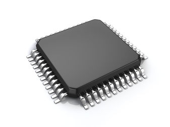
The MB9BF120 is a highly integrated 32-bit microcontrollers dedicated for embedded controllers with low-power consumption mode and competitive cost. These series are based on the ARM Cortex-M3 Processor with on-chip Flash memory and SRAM, and have peripheral functions such as various timers, ADCs, DACs and Communication Interfaces (UART, CSIO, I2C, LIN).
- 32-bit ARM Cortex-M3 Core
- Processor version: r2p1
- Up to 72 MHz Frequency Operation
- Integrated Nested Vectored Interrupt Controller (NVIC): 1 NMI (non-maskable interrupt) and 48 peripheral interrupts and 16 priority levels
- 24-bit System timer (Sys Tick): System timer for OS task management
- On-chip Memories
- Flash memory
- SRAM
- Multi-function Serial Interface (Max eight channels)
- DMA Controller (Eight channels)
- 8 independently configured and operated channels
- Transfer can be started by software or request from the built-in peripherals
- Transfer address area: 32-bit (4 Gbytes)
- Transfer mode: Block transfer/Burst transfer/Demand transfer
- Transfer data type: byte/half-word/word
- Transfer block count: 1 to 16
- Number of transfers: 1 to 65536
- A/D Converter (Max 26 channels)
- Successive Approximation type
- Built-in 2units
- Conversion time: 0.8 µs @ 5 V
- Priority conversion available (priority at 2 levels)
- Scanning conversion mode
- Built-in FIFO for conversion data storage (for SCAN conversion: 16 steps, for Priority conversion: 4 steps)
- D/A Converter (Max two channels)
- R-2R type
- 10-bit resolution
- Base Timer (Max eight channels)
- 16-bit PWM timer
- 16-bit PPG timer
- 16-/32-bit reload timer
- 16-/32-bit PWC timer
- General-Purpose I/O Port
- Capable of pull-up control per pin
- Capable of reading pin level directly
- Built-in the port relocate function
- Up to 65 high-speed general-purpose I/O Ports @ 80 pin Package
- Some ports are 5 V tolerant.
- Dual Timer (32-/16-bit Down Counter)
- Free-running
- Periodic (=Reload)
- One-shot
- Quadrature Position/Revolution Counter (QPRC) (Max two channels)
- Multi-function Timer
- Real-time clock (RTC)
- Watch Counter
- External Interrupt Controller Unit
- Watchdog Timer (Two channels)
- CRC (Cyclic Redundancy Check) Accelerator
- Clock and Reset
- Clock Super Visor (CSV)
- Low-Voltage Detector (LVD)
- Low-Power Consumption Mode
- Debug – Serial Wire JTAG Debug Port (SWJ-DP)
- Unique ID – Unique value of the device (41 bits) is set
- Power Supply – Wide range voltage: VCC = 2.7 V to 5.5 V