Описание
The NXP LPC3141 combine a 270 MHz ARM926EJ-S CPU core, High-speed USB 2.0 OTG, 192 KB SRAM, NAND flash controller, flexible external bus interface, four channel 10-bit A/D, and a myriad of serial and parallel interfaces in a single chip targeted at consumer, industrial, medical, and communication markets. To optimize system power consumption, the LPC3141/3143 have multiple power domains and a very flexible Clock Generation Unit (CGU) that provides dynamic clock gating and scaling.
- CPU platform
- 270 MHz, 32-bit ARM926EJ-S
- 16 kB D-cache and 16 kB I-cache
- Memory Management Unit (MMU)
- Internal memory
- 192 kB embedded SRAM
- External memory interface
- NAND flash controller with 8-bit ECC and AES decryption support (LPC3143 only)
- 8/16-bit Multi-Port Memory Controller (MPMC): SDRAM and SRAM
- Security
- AES decryption engine (LPC3143 only)
- Secure one-time programmable memory for AES key storage and customer use
- 128 bit unique ID per device for DRM schemes
- Communication and connectivity
- High-speed USB 2.0 (OTG, Host, Device) with on-chip PHY
- Two I2S interfaces
- Integrated master/slave SPI
- Two master/slave I2C-bus interfaces
- Fast UART
- Memory Card Interface (MCI): MMC/SD/SDIO/CE-ATA
- Four-channel 10-bit ADC
- Integrated 4/8/16-bit 6800/8080 compatible LCD interface
- System functions
- Dynamic clock gating and scaling
- Multiple power domains
- Selectable boot-up: SPI flash, NAND flash, SD/MMC cards, UART, or USB
- On the LPC3143 only: secure booting using an AES decryption engine from SPI flash, NAND flash, SD/MMC cards, UART, or USB.
- DMA controller
- Four 32-bit timers
- Watchdog timer
- PWM module
- Master/slave PCM interface
- Random Number Generator (RNG)
- General Purpose I/O pins (GPIO)
- Flexible and versatile interrupt structure
- JTAG interface with boundary scan and ARM debug access
- Operating voltage and temperature
- Core voltage: 1.2 V
- I/O voltages: 1.8 V, 3.3 V
- Temperature: -40°C to +85°C
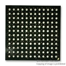
- TFBGA180 package: 12 x 12 mm, 0.8 mm pitch