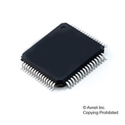
MCU 32-bit LPC11E00 ARM Cortex M0 RISC 128KB Flash 3.3V 64-Pin LQFP Tray, LPC11E37FBD64/501E, NXP

The LPC11E3x are a ARM Cortex-M0 based, low-cost 32-bit MCU family, designed for 8/16-bit microcontroller applications, offering performance, low power, simple instruction set and memory addressing together with reduced code size compared to existing 8/16-bit architectures. The LPC11E3x operate at CPU frequencies of up to 50 MHz. The peripheral complement of the LPC11E3x includes up to 128 kB of flash memory, up to 12 kB of SRAM data memory and 4 kB EEPROM, one Fast-mode Plus I²C-bus interface, one RS-485/EIA-485 USART with support for synchronous mode and smart card interface, two SSP interfaces, four general purpose counter/timers, a 10-bit ADC, and up to 54 general purpose I/O pins.

  • System:
    • ARM Cortex-M0 processor, running at frequencies of up to 50 MHz.
    • ARM Cortex-M0 built-in Nested Vectored Interrupt Controller (NVIC).
    • Non Maskable Interrupt (NMI) input selectable from several input sources.
    • System tick timer.
  • Memory:
    • Up to 128 kB on-chip flash program memory with sector (4 kB) and page erase(256 byte) access.
    • 4 kB on-chip EEPROM data memory; byte erasable and byte programmable;on-chip API support.
    • 12 kB SRAM data memory.
    • 16 kB boot ROM.
    • In-System Programming (ISP) and In-Application Programming (IAP) via on-chipbootloader software.
    • ROM-based 32-bit integer division routines.
  • Debug options:
    • Standard JTAG (Joint Test Action Group) test interface for BSDL (Boundary ScanDescription Language).
    • Serial Wire Debug.
  • Digital peripherals:
    • Up to 54 General Purpose I/O (GPIO) pins with configurable pull-up/pull-downresistors, repeater mode, and open-drain mode.
    • Up to 8 GPIO pins can be selected as edge and level sensitive interrupt sources.
    • Two GPIO grouped interrupt modules enable an interrupt based on aprogrammable pattern of input states of a group of GPIO pins.
    • High-current source output driver (20 mA) on one pin.
    • High-current sink driver (20 mA) on true open-drain pins.
    • Four general purpose counter/timers with a total of up to 8 capture inputs and 13match outputs.
    • Programmable Windowed WatchDog Timer (WWDT) with a dedicated, internallow-power WatchDog Oscillator (WDO).
  • Analog peripherals:
    • 10-bit ADC with input multiplexing among eight pins.
  • Serial interfaces:
    • USART with fractional baud rate generation, internal FIFO, a full modem controlhandshake interface, and support for RS-485/9-bit mode and synchronous mode.USART supports an asynchronous smart card interface (ISO 7816-3).
    • Two SSP controllers with FIFO and multi-protocol capabilities.
    • I²C-bus interface supporting the full I²C-bus specification and Fast-mode Plus witha data rate of up to 1 Mbit/s with multiple address recognition and monitor mode.
  • Clock generation:
    • Crystal Oscillator with an operating range of 1 MHz to 25 MHz (system oscillator).
    • 12 MHz high-frequency Internal RC oscillator (IRC) that can optionally be used asa system clock.
    • Internal low-power, low-frequency WatchDog Oscillator (WDO) with programmablefrequency output.
    • PLL allows CPU operation up to the maximum CPU rate with the system oscillatoror the IRC as clock sources.
    • Clock output function with divider that can reflect the crystal oscillator, the mainclock, the IRC, or the watchdog oscillator.
  • Power control:
    • Integrated PMU (Power Management Unit) to minimize power consumption duringSleep, Deep-sleep, Power-down, and Deep power-down modes.
    • Power profiles residing in boot ROM provide optimized performance and minimizedpower consumption for any given application through one simple function call.
    • Four reduced power modes: Sleep, Deep-sleep, Power-down, and Deeppower-down.
    • Processor wake-up from Deep-sleep and Power-down modes via reset, selectableGPIO pins, or the watchdog interrupt.
    • Processor wake-up from Deep power-down mode using one special function pin.
    • Power-On Reset (POR).
    • Brownout detect with four separate thresholds for interrupt and forced reset.
  • Unique device serial number for identification.
  • Single 3.3 V power supply (1.8 V to 3.6 V).
  • Temperature range -40 °C to +85 °C.
  • Available as LQFP64, LQFP48, and HVQFN33 packages.
Характеристики

Program_memory_type

Flash

Supplier_package

LQFP

Specifications

https://4donline.ihs.com/images/VipMasterIC/IC/PHGL/PHGLS25742/PHGLS25742-1.pdf?hkey=52A5661711E402568146F3353EA87419

Schedule_b

8542310000

Ram_size

12 KB

Program_memory_size

128 KB

Product_dimensions

10.1 x 10.1 x 1.4 mm

Pin_count

64

Operating_temperature

-40 to 85 °C

Operating_supply_voltage

3.3 V

Watchdog

1

Eccn

EAR99

Instruction_set_architecture

RISC

Htsn

8542310001

Тип интерфейса

I2C/UART

Device_core

ARM Cortex M0

Data_bus_width

32 Bit

Country_of_origin

Taiwan

Бренд

On_chip_adc

8-chx10-bit

Min_operating_supply_voltage

1.8 V

Number_of_timers

4

Number_of_programmable_i_os

54

Msl_level

2

Mounting

Surface Mount

Max_speed

50 MHz

Max_power_dissipation

1500 mW

Max_operating_supply_voltage

3.6 V

Артикул: LPC11E37FBD64/501E

Описание

The LPC11E3x are a ARM Cortex-M0 based, low-cost 32-bit MCU family, designed for 8/16-bit microcontroller applications, offering performance, low power, simple instruction set and memory addressing together with reduced code size compared to existing 8/16-bit architectures. The LPC11E3x operate at CPU frequencies of up to 50 MHz. The peripheral complement of the LPC11E3x includes up to 128 kB of flash memory, up to 12 kB of SRAM data memory and 4 kB EEPROM, one Fast-mode Plus I²C-bus interface, one RS-485/EIA-485 USART with support for synchronous mode and smart card interface, two SSP interfaces, four general purpose counter/timers, a 10-bit ADC, and up to 54 general purpose I/O pins.

  • System:
    • ARM Cortex-M0 processor, running at frequencies of up to 50 MHz.
    • ARM Cortex-M0 built-in Nested Vectored Interrupt Controller (NVIC).
    • Non Maskable Interrupt (NMI) input selectable from several input sources.
    • System tick timer.
  • Memory:
    • Up to 128 kB on-chip flash program memory with sector (4 kB) and page erase(256 byte) access.
    • 4 kB on-chip EEPROM data memory; byte erasable and byte programmable;on-chip API support.
    • 12 kB SRAM data memory.
    • 16 kB boot ROM.
    • In-System Programming (ISP) and In-Application Programming (IAP) via on-chipbootloader software.
    • ROM-based 32-bit integer division routines.
  • Debug options:
    • Standard JTAG (Joint Test Action Group) test interface for BSDL (Boundary ScanDescription Language).
    • Serial Wire Debug.
  • Digital peripherals:
    • Up to 54 General Purpose I/O (GPIO) pins with configurable pull-up/pull-downresistors, repeater mode, and open-drain mode.
    • Up to 8 GPIO pins can be selected as edge and level sensitive interrupt sources.
    • Two GPIO grouped interrupt modules enable an interrupt based on aprogrammable pattern of input states of a group of GPIO pins.
    • High-current source output driver (20 mA) on one pin.
    • High-current sink driver (20 mA) on true open-drain pins.
    • Four general purpose counter/timers with a total of up to 8 capture inputs and 13match outputs.
    • Programmable Windowed WatchDog Timer (WWDT) with a dedicated, internallow-power WatchDog Oscillator (WDO).
  • Analog peripherals:
    • 10-bit ADC with input multiplexing among eight pins.
  • Serial interfaces:
    • USART with fractional baud rate generation, internal FIFO, a full modem controlhandshake interface, and support for RS-485/9-bit mode and synchronous mode.USART supports an asynchronous smart card interface (ISO 7816-3).
    • Two SSP controllers with FIFO and multi-protocol capabilities.
    • I²C-bus interface supporting the full I²C-bus specification and Fast-mode Plus witha data rate of up to 1 Mbit/s with multiple address recognition and monitor mode.
  • Clock generation:
    • Crystal Oscillator with an operating range of 1 MHz to 25 MHz (system oscillator).
    • 12 MHz high-frequency Internal RC oscillator (IRC) that can optionally be used asa system clock.
    • Internal low-power, low-frequency WatchDog Oscillator (WDO) with programmablefrequency output.
    • PLL allows CPU operation up to the maximum CPU rate with the system oscillatoror the IRC as clock sources.
    • Clock output function with divider that can reflect the crystal oscillator, the mainclock, the IRC, or the watchdog oscillator.
  • Power control:
    • Integrated PMU (Power Management Unit) to minimize power consumption duringSleep, Deep-sleep, Power-down, and Deep power-down modes.
    • Power profiles residing in boot ROM provide optimized performance and minimizedpower consumption for any given application through one simple function call.
    • Four reduced power modes: Sleep, Deep-sleep, Power-down, and Deeppower-down.
    • Processor wake-up from Deep-sleep and Power-down modes via reset, selectableGPIO pins, or the watchdog interrupt.
    • Processor wake-up from Deep power-down mode using one special function pin.
    • Power-On Reset (POR).
    • Brownout detect with four separate thresholds for interrupt and forced reset.
  • Unique device serial number for identification.
  • Single 3.3 V power supply (1.8 V to 3.6 V).
  • Temperature range -40 °C to +85 °C.
  • Available as LQFP64, LQFP48, and HVQFN33 packages.
Детали

Program_memory_type

Flash

Supplier_package

LQFP

Specifications

https://4donline.ihs.com/images/VipMasterIC/IC/PHGL/PHGLS25742/PHGLS25742-1.pdf?hkey=52A5661711E402568146F3353EA87419

Schedule_b

8542310000

Ram_size

12 KB

Program_memory_size

128 KB

Product_dimensions

10.1 x 10.1 x 1.4 mm

Pin_count

64

Operating_temperature

-40 to 85 °C

Operating_supply_voltage

3.3 V

Watchdog

1

Eccn

EAR99

Instruction_set_architecture

RISC

Htsn

8542310001

Тип интерфейса

I2C/UART

Device_core

ARM Cortex M0

Data_bus_width

32 Bit

Country_of_origin

Taiwan

Бренд

On_chip_adc

8-chx10-bit

Min_operating_supply_voltage

1.8 V

Number_of_timers

4

Number_of_programmable_i_os

54

Msl_level

2

Mounting

Surface Mount

Max_speed

50 MHz

Max_power_dissipation

1500 mW

Max_operating_supply_voltage

3.6 V