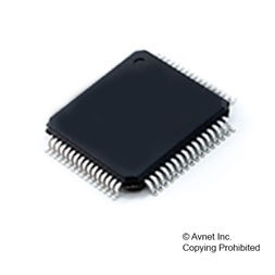
MCU 32-Bit KV10 ARM Cortex M0+ RISC 128KB Flash 1.8V/2.5V/3.3V 64-Pin LQFP Tray, MKV10Z128VLH7, NXP

The Kinetis V Series KV11x MCU family is built on ARM CortexM0+ core and enabled by innovative 90nm thin film storage (TFS) flash process technology. The KV11x is an extension of the existing KV10x family providing increased memory, higher pin count, additional FTMs and a FlexCAN serial interface. KV11x is ideal for industrial motor control applications, inverters, and low-end power conversion applications.

  • Performance
    • Up to 75 MHz ARM Cortex-M0+ based core
  • Memories and memory interfaces
    • Up to 128 KB of program flash memory
    • Up to 16 KB of RAM
  • System peripherals
    • Nine low-power modes to provide power optimization based on application requirements
    • 8-channel DMA controller
    • SWD interface and Micro Trace buffer
    • Bit Manipulation Engine (BME)
    • External watchdog timer
    • Advanced independent clocked watchdog
    • Memory Mapped Divide and Square Root (MMDVSQ) module
  • Clocks
    • 32-40 kHz or 4-32 MHz external crystal oscillator
    • Multipurpose clock generator (MCG) with frequencylocked loop referencing either internal or external reference clock
  • Security and integrity modules
    • 80-bit unique identification (ID) number per chip
    • Hardware CRC module
  • Communication interfaces
    • One 16-bit SPI module
    • One I²C module
    • Two UART modules
    • One FlexCAN module1
  • Timers
    • Programmable delay block
    • Two 6-channel FlexTimers (FTM) for motor control/ general purpose applications
    • Four 2-channel FlexTimers (FTM) with quadrature decoder functionality
    • 16-bit low-power timer (LPTMR)
  • Operating Characteristics
    • Voltage range: 1.71 to 3.6 V
    • Flash write voltage range: 1.71 to 3.6 V
    • Temperature range (ambient): –40 to 105°C
  • Analog modules
    • Two 16-bit SAR ADCs
    • 12-bit DAC
    • Two analog comparators (ACMP) containing a 6-bit DAC and programmable reference input
  • Human-machine interface
    • General-purpose I/O

Характеристики

Program_memory_type

Flash

Supplier_package

LQFP

Specifications

https://4donline.ihs.com/images/VipMasterIC/IC/PHGL/PHGL-S-A0003205394/PHGL-S-A0003205394-1.pdf?hkey=52A5661711E402568146F3353EA87419

Screening_level

Extended Industrial

Schedule_b

8542390000

Ram_size

16 Kb

Program_memory_size

128 KB

Product_dimensions

10 x 10 x 1.4

Pin_count

64

Operating_temperature

-40 to 105 °C

Operating_supply_voltage

1.8, 2.5, 3.3 V

Watchdog

1

Analog_comparators

2

Eccn

3A991.A.2

Instruction_set_architecture

RISC

Htsn

8542310001

Тип интерфейса

I2C/SPI/UART

Device_core

ARM Cortex M0+

Data_bus_width

32 Bit

Country_of_origin

China

Бренд

Min_operating_supply_voltage

1.71 V

Number_of_timers

7

Number_of_programmable_i_os

54

Msl_level

3

Mounting

Surface Mount

Max_speed

75 MHz

Max_processing_temp

260 °C

Max_operating_supply_voltage

3.6 V

Lead_finish

Matte Tin

Артикул: MKV10Z128VLH7

Описание

The Kinetis V Series KV11x MCU family is built on ARM CortexM0+ core and enabled by innovative 90nm thin film storage (TFS) flash process technology. The KV11x is an extension of the existing KV10x family providing increased memory, higher pin count, additional FTMs and a FlexCAN serial interface. KV11x is ideal for industrial motor control applications, inverters, and low-end power conversion applications.

  • Performance
    • Up to 75 MHz ARM Cortex-M0+ based core
  • Memories and memory interfaces
    • Up to 128 KB of program flash memory
    • Up to 16 KB of RAM
  • System peripherals
    • Nine low-power modes to provide power optimization based on application requirements
    • 8-channel DMA controller
    • SWD interface and Micro Trace buffer
    • Bit Manipulation Engine (BME)
    • External watchdog timer
    • Advanced independent clocked watchdog
    • Memory Mapped Divide and Square Root (MMDVSQ) module
  • Clocks
    • 32-40 kHz or 4-32 MHz external crystal oscillator
    • Multipurpose clock generator (MCG) with frequencylocked loop referencing either internal or external reference clock
  • Security and integrity modules
    • 80-bit unique identification (ID) number per chip
    • Hardware CRC module
  • Communication interfaces
    • One 16-bit SPI module
    • One I²C module
    • Two UART modules
    • One FlexCAN module1
  • Timers
    • Programmable delay block
    • Two 6-channel FlexTimers (FTM) for motor control/ general purpose applications
    • Four 2-channel FlexTimers (FTM) with quadrature decoder functionality
    • 16-bit low-power timer (LPTMR)
  • Operating Characteristics
    • Voltage range: 1.71 to 3.6 V
    • Flash write voltage range: 1.71 to 3.6 V
    • Temperature range (ambient): –40 to 105°C
  • Analog modules
    • Two 16-bit SAR ADCs
    • 12-bit DAC
    • Two analog comparators (ACMP) containing a 6-bit DAC and programmable reference input
  • Human-machine interface
    • General-purpose I/O

Детали

Program_memory_type

Flash

Supplier_package

LQFP

Specifications

https://4donline.ihs.com/images/VipMasterIC/IC/PHGL/PHGL-S-A0003205394/PHGL-S-A0003205394-1.pdf?hkey=52A5661711E402568146F3353EA87419

Screening_level

Extended Industrial

Schedule_b

8542390000

Ram_size

16 Kb

Program_memory_size

128 KB

Product_dimensions

10 x 10 x 1.4

Pin_count

64

Operating_temperature

-40 to 105 °C

Operating_supply_voltage

1.8, 2.5, 3.3 V

Watchdog

1

Analog_comparators

2

Eccn

3A991.A.2

Instruction_set_architecture

RISC

Htsn

8542310001

Тип интерфейса

I2C/SPI/UART

Device_core

ARM Cortex M0+

Data_bus_width

32 Bit

Country_of_origin

China

Бренд

Min_operating_supply_voltage

1.71 V

Number_of_timers

7

Number_of_programmable_i_os

54

Msl_level

3

Mounting

Surface Mount

Max_speed

75 MHz

Max_processing_temp

260 °C

Max_operating_supply_voltage

3.6 V

Lead_finish

Matte Tin