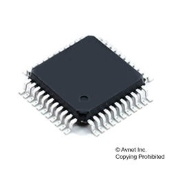
MCU 32-Bit KE06 ARM Cortex M0+ RISC 128KB Flash 3.3V/5V 44-Pin LQFP Tray, MKE06Z128VLD4, NXP

The Kinetis KE06 MCU family delivers a next-generation solution with enhanced ESD/EMC performance for cost-sensitive, high-reliability device applications used in high electrical noise environments. Offers a cost-effective, entry-level 32-bit solution featuring low power and high robustness Provides a pin-compatibility within the Kinetis E series portfolio, as well as pin compatibility with Freescale"s 8-bit S08P family Includes a powerful array of analog, communication and timing, and control peripherals with varying flash memory size and pin count

Operating characteristics

  • Voltage range: 2.7 to 5.5 V
  • Flash write voltage range: 2.7 to 5.5 V
  • Temperature range (ambient): -40 to 105°C

Performance

  • Up to 48 MHz ARM® Cortex®-M0+ core
  • Single cycle 32-bit x 32-bit multiplier
  • Single cycle I/O access port

Memories and memory interfaces

  • Up to 128 KB flash
  • Up to 256 B EEPROM
  • Up to 16 KB RAM

Clocks

  • Oscillator (OSC) – loop-controlled Pierce oscillator, crystal or ceramic resonator range of 31.25 kHz to 39.0625 kHz or 4 MHz to 20 MHz
  • Internal clock source (ICS) – internal FLL with internal or external reference, precision trimming of internal reference allowing 1% deviation across temperature range of 0 °C to 70 °C and 1.5% deviation across temperature range of -40 °C to 105 °C, up to 20 MHz
  • Internal 1 kHz low-power oscillator (LPO)

System peripherals

  • Power management module (PMC) with three power modes: run, wait, stop
  • Low-voltage detection (LVD) with reset or interrupt, selectable trip points
  • Watchdog with independent clock source (WDOG)
  • Programmable cyclic redundancy check module (CRC)
  • Serial wire debug interface (SWD)
  • Bit manipulation engine (BME)

Security and integrity modules

  • 64-bit unique identification (ID) number per chip

Human-machine interface

  • Up to 71 general-purpose input/output (GPIO)
  • Two 8-bit keyboard interrupt modules (KBI)

Analog modules

  • One 16-channel 12-bit SAR ADC with internal band gap reference channel, operation in Stop mode, optional hardware trigger (ADC)
  • Two analog comparators containing a 6-bit DAC and programmable reference input (ACMP)

Timers

  • One 6-channel FlexTimer/PWM (FTM)
  • Two 2-channel FlexTimer/PWM (FTM)
  • One 2-channel periodic interrupt timer (PIT)
  • One real-time clock (RTC)
  • One pulse-width timer (PWT)
  • One fast timer

Connectivity and Communications

  • Three SCI (LIN capable)
  • Two I²C compatible with SMBus V2 features
  • Two 8-bit SPI
  • One CAN module

Характеристики

Program_memory_type

Flash

Supplier_package

LQFP

Specifications

https://4donline.ihs.com/images/VipMasterIC/IC/PHGL/PHGL-L-A0007335111/PHGL-S-A0007324880-1.pdf?hkey=52A5661711E402568146F3353EA87419

Special_features

CAN Controller

Schedule_b

8542310000

Ram_size

16 Kb

Program_memory_size

128 KB

Product_dimensions

10 x 10 x 1.4

Pin_count

44

Operating_temperature

-40 to 105 °C

Operating_supply_voltage

3.3, 5 V

Watchdog

1

Analog_comparators

2

Eccn

3A991.A.2

Instruction_set_architecture

RISC

Htsn

8542310001

Тип интерфейса

CAN/I2C/SPI/UART

Device_core

ARM Cortex M0+

Data_bus_width

32 Bit

Country_of_origin

China

Бренд

On_chip_adc

16-chx12-bit

Min_operating_supply_voltage

2.7 V

Number_of_timers

5

Number_of_programmable_i_os

38

Msl_level

3

Mounting

Surface Mount

Max_speed

48 MHz

Max_processing_temp

260 °C

Max_operating_supply_voltage

5.5 V

Lead_finish

Matte Tin

Артикул: MKE06Z128VLD4

Описание

The Kinetis KE06 MCU family delivers a next-generation solution with enhanced ESD/EMC performance for cost-sensitive, high-reliability device applications used in high electrical noise environments. Offers a cost-effective, entry-level 32-bit solution featuring low power and high robustness Provides a pin-compatibility within the Kinetis E series portfolio, as well as pin compatibility with Freescale"s 8-bit S08P family Includes a powerful array of analog, communication and timing, and control peripherals with varying flash memory size and pin count

Operating characteristics

  • Voltage range: 2.7 to 5.5 V
  • Flash write voltage range: 2.7 to 5.5 V
  • Temperature range (ambient): -40 to 105°C

Performance

  • Up to 48 MHz ARM® Cortex®-M0+ core
  • Single cycle 32-bit x 32-bit multiplier
  • Single cycle I/O access port

Memories and memory interfaces

  • Up to 128 KB flash
  • Up to 256 B EEPROM
  • Up to 16 KB RAM

Clocks

  • Oscillator (OSC) – loop-controlled Pierce oscillator, crystal or ceramic resonator range of 31.25 kHz to 39.0625 kHz or 4 MHz to 20 MHz
  • Internal clock source (ICS) – internal FLL with internal or external reference, precision trimming of internal reference allowing 1% deviation across temperature range of 0 °C to 70 °C and 1.5% deviation across temperature range of -40 °C to 105 °C, up to 20 MHz
  • Internal 1 kHz low-power oscillator (LPO)

System peripherals

  • Power management module (PMC) with three power modes: run, wait, stop
  • Low-voltage detection (LVD) with reset or interrupt, selectable trip points
  • Watchdog with independent clock source (WDOG)
  • Programmable cyclic redundancy check module (CRC)
  • Serial wire debug interface (SWD)
  • Bit manipulation engine (BME)

Security and integrity modules

  • 64-bit unique identification (ID) number per chip

Human-machine interface

  • Up to 71 general-purpose input/output (GPIO)
  • Two 8-bit keyboard interrupt modules (KBI)

Analog modules

  • One 16-channel 12-bit SAR ADC with internal band gap reference channel, operation in Stop mode, optional hardware trigger (ADC)
  • Two analog comparators containing a 6-bit DAC and programmable reference input (ACMP)

Timers

  • One 6-channel FlexTimer/PWM (FTM)
  • Two 2-channel FlexTimer/PWM (FTM)
  • One 2-channel periodic interrupt timer (PIT)
  • One real-time clock (RTC)
  • One pulse-width timer (PWT)
  • One fast timer

Connectivity and Communications

  • Three SCI (LIN capable)
  • Two I²C compatible with SMBus V2 features
  • Two 8-bit SPI
  • One CAN module

Детали

Program_memory_type

Flash

Supplier_package

LQFP

Specifications

https://4donline.ihs.com/images/VipMasterIC/IC/PHGL/PHGL-L-A0007335111/PHGL-S-A0007324880-1.pdf?hkey=52A5661711E402568146F3353EA87419

Special_features

CAN Controller

Schedule_b

8542310000

Ram_size

16 Kb

Program_memory_size

128 KB

Product_dimensions

10 x 10 x 1.4

Pin_count

44

Operating_temperature

-40 to 105 °C

Operating_supply_voltage

3.3, 5 V

Watchdog

1

Analog_comparators

2

Eccn

3A991.A.2

Instruction_set_architecture

RISC

Htsn

8542310001

Тип интерфейса

CAN/I2C/SPI/UART

Device_core

ARM Cortex M0+

Data_bus_width

32 Bit

Country_of_origin

China

Бренд

On_chip_adc

16-chx12-bit

Min_operating_supply_voltage

2.7 V

Number_of_timers

5

Number_of_programmable_i_os

38

Msl_level

3

Mounting

Surface Mount

Max_speed

48 MHz

Max_processing_temp

260 °C

Max_operating_supply_voltage

5.5 V

Lead_finish

Matte Tin