Описание
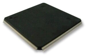
The STM32F767xx devices are based on the high-performance ARM Cortex-M7 32-bit RISC core operating at up to 216 MHz frequency. The Cortex-M7 core features a floating point unit (FPU) which supports ARM double-precision and single-precision data-processing instructions and data types. It also implements a full set of DSP instructions and a memory protection unit (MPU) which enhances the application security. The STM32F767xx devices incorporate high-speed embedded memories with a Flash memory up to 2 Mbytes, 512 Kbytes of SRAM (including 128 Kbytes of Data TCM RAM for critical real-time data), 16 Kbytes of instruction TCM RAM (for critical real-time routines), 4 Kbytes of backup SRAM available in the lowest power modes, and an extensive range of enhanced I/Os and peripherals connected to two APB buses, two AHB buses, a 32-bit multi-AHB bus matrix and a multi layer AXI interconnect supporting internal and external memories access. All the devices offer three 12-bit ADCs, two DACs, a low-power RTC, twelve generalpurpose 16-bit timers including two PWM timers for motor control, two general-purpose 32- bit timers, a true random number generator (RNG). They also feature standard and advanced communication interfaces. The STM32F767xx devices operate in the –40°C to +105°C temperature range from a 1.7 to 3.6 V power supply. Dedicated supply inputs for USB (OTG_FS and OTG_HS) and SDMMC2 (clock, command and 4-bit data) are available on all the packages except LQFP100 for a greater power supply choice.
- Core: ARM® 32-bit Cortex®-M7 CPU with DPFPU, ART Accelerator™ and L1-cache: 16 Kbytes I/D cache, allowing 0-wait state execution from embedded Flash and external memories, up to 216 MHz, MPU, 462 DMIPS/2.14 DMIPS/MHz (Dhrystone 2.1), and DSP instructions.
- Memories
- Up to 2 Mbytes of Flash memory organized into two banks allowing read-while-write
- SRAM: 512 Kbytes (including 128 Kbytes of data TCM RAM for critical real-time data) + 16 Kbytes of instruction TCM RAM (for critical real-time routines) + 4 Kbytes of backup SRAM
- Flexible external memory controller with up to 32-bit data bus: SRAM, PSRAM, SDRAM/LPSDR SDRAM, NOR/NAND memories
- Dual mode Quad-SPI
- Graphics
- Chrom-ART Accelerator™ (DMA2D), graphical hardware accelerator enabling enhanced graphical user interface
- Hardware JPEG codec
- LCD-TFT controller supporting up to XGA resolution
- MIPI® DSI host controller supporting up to 720p 30 Hz resolution
- Clock, reset and supply management
- 1.7 V to 3.6 V application supply and I/Os
- POR, PDR, PVD and BOR
- Dedicated USB power
- 4-to-26 MHz crystal oscillator
- Internal 16 MHz factory-trimmed RC (1% accuracy)
- 32 kHz oscillator for RTC with calibration
- Internal 32 kHz RC with calibration
- Low-power
- Sleep, Stop and Standby modes
- VBAT supply for RTC, 32×32 bit backup registers + 4 Kbytes backup SRAM
- 3×12-bit, 2.4 MSPS ADC: up to 24 channels
- Digital filters for sigma delta modulator (DFSDM), 8 channels / 4 filters
- 2×12-bit D/A converters
- General-purpose DMA: 16-stream DMA controller with FIFOs and burst support
- Up to 18 timers: up to thirteen 16-bit (1x lowpower 16-bit timer available in Stop mode) and two 32-bit timers, each with up to 4 IC/OC/PWM or pulse counter and quadrature (incremental) encoder input. All 15 timers running up to 216 MHz. 2x watchdogs, SysTick timer
- Debug mode
- SWD & JTAG interfaces
- Cortex®-M7 Trace Macrocell™
- Up to 168 I/O ports with interrupt capability
- Up to 164 fast I/Os up to 108 MHz
- Up to 166 5 V-tolerant I/Os
