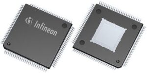
MCU 16-Bit XE166 C166 V2 CISC/DSP/RISC 320KB Flash 1.5V/3.3V/5V 100-Pin LQFP T/R, XE164FN40F80LRABKXUMA1, Infineon

The XE162N (LQFP-64) and XE164N (LQFP-100) microcontroller series is based on Infineon"s popular and well-established C166 architecture.

  • High-performance CPU with five-stage pipeline and MPU
    • 12.5 ns instruction cycle @ 80 MHz CPU clock (single-cycle execution)
    • One-cycle 32-bit addition and subtraction with 40-bit result
    • One-cycle multiplication (16 × 16 bit)
    • Background division (32 / 16 bit) in 21 cycles
    • One-cycle multiply-and-accumulate (MAC) instructions
    • Enhanced Boolean bit manipulation facilities
    • Zero-cycle jump execution
    • Additional instructions to support HLL and operating systems
    • Register-based design with multiple variable register banks
    • Fast context switching support with two additional local register banks
    • 16 Mbytes total linear address space for code and data
    • 1,024 Bytes on-chip special function register area (C166 Family compatible)
    • Integrated Memory Protection Unit (MPU)
  • Interrupt system with 16 priority levels providing 96 interrupt nodes
    • Selectable external inputs for interrupt generation and wake-up
    • Fastest sample-rate 12.5 ns
  • Eight-channel interrupt-driven single-cycle data transfer with Peripheral Event Controller (PEC), 24-bit pointers cover total address space
  • Clock generation from internal or external clock sources, using on-chip PLL or prescaler
  • Hardware CRC-Checker with Programmable Polynomial to Supervise On-Chip Memory Areas
  • On-chip memory modules
    • 8 Kbytes on-chip stand-by RAM (SBRAM)
    • 2 Kbytes on-chip dual-port RAM (DPRAM)
    • Up to 16 Kbytes on-chip data SRAM (DSRAM)
    • Up to 16 Kbytes on-chip program/data SRAM (PSRAM)
    • Up to 320 Kbytes on-chip program memory (Flash memory)
    • Memory content protection through Error Correction Code (ECC)
  • On-Chip Peripheral Modules
    • Two synchronizable A/D Converters with up to 16 channels, 10-bit resolution, conversion time below 1 µs, optional data preprocessing (data reduction, range check), broken wire detection
    • 16-channel general purpose capture/compare unit (CC2)
    • Two capture/compare units for flexible PWM signal generation (CCU6x)
    • Multi-functional general purpose timer unit with 5 timers
    • Up to 6 serial interface channels to be used as UART, LIN, high-speed synchronous channel (SPI/QSPI), IIC bus interface (10-bit addressing, 400 kbit/s), IIS interface
    • On-chip MultiCAN interface (Rev. 2.0B active) with 64 message objects (Full CAN/Basic CAN) on up to 2 CAN nodes and gateway functionality
    • On-chip system timer and on-chip real time clock
  • Up to 12 Mbytes external address space for code and data
    • Programmable external bus characteristics for different address ranges
    • Multiplexed or demultiplexed external address/data buses
    • Selectable address bus width

Характеристики

Schedule_b

8542310000

Operating_supply_voltage

1.5, 3.3, 5 V

Operating_temperature

-40 to 125 °C

Pin_count

100

Product_dimensions

14 x 14 x 1.4 mm

Program_memory_size

40 KB

Program_memory_type

Flash

Ram_size

5.25 KB

Screening_level

Automotive

On_chip_adc

16-chx10-bit

Special_features

CAN Controller

Specifications

http://www.infineon.com/dgdl/Infineon-XE164XN-DS-v01_04-en.pdf?fileId=db3a30432313ff5e01235220469362ff

Supplier_package

LQFP

Watchdog

2

Max_speed

80 MHz

Number_of_timers

5

Бренд

Instruction_set_architecture

CISC, DSP, RISC

Data_bus_width

16 Bit

Device_core

C166 V2

Eccn

3A991.A.2

Htsn

8542310001

Тип интерфейса

CAN/I2C/I2S/SPI/UART

Number_of_programmable_i_os

75

Lead_finish

Tin

Max_expanded_memory_size

16 MB

Max_operating_supply_voltage

5.5 V

Max_power_dissipation

800 mW

Min_operating_supply_voltage

3 V

Mounting

Surface Mount

Msl_level

3

Артикул: XE164FN40F80LRABKXUMA1

Описание

The XE162N (LQFP-64) and XE164N (LQFP-100) microcontroller series is based on Infineon"s popular and well-established C166 architecture.

  • High-performance CPU with five-stage pipeline and MPU
    • 12.5 ns instruction cycle @ 80 MHz CPU clock (single-cycle execution)
    • One-cycle 32-bit addition and subtraction with 40-bit result
    • One-cycle multiplication (16 × 16 bit)
    • Background division (32 / 16 bit) in 21 cycles
    • One-cycle multiply-and-accumulate (MAC) instructions
    • Enhanced Boolean bit manipulation facilities
    • Zero-cycle jump execution
    • Additional instructions to support HLL and operating systems
    • Register-based design with multiple variable register banks
    • Fast context switching support with two additional local register banks
    • 16 Mbytes total linear address space for code and data
    • 1,024 Bytes on-chip special function register area (C166 Family compatible)
    • Integrated Memory Protection Unit (MPU)
  • Interrupt system with 16 priority levels providing 96 interrupt nodes
    • Selectable external inputs for interrupt generation and wake-up
    • Fastest sample-rate 12.5 ns
  • Eight-channel interrupt-driven single-cycle data transfer with Peripheral Event Controller (PEC), 24-bit pointers cover total address space
  • Clock generation from internal or external clock sources, using on-chip PLL or prescaler
  • Hardware CRC-Checker with Programmable Polynomial to Supervise On-Chip Memory Areas
  • On-chip memory modules
    • 8 Kbytes on-chip stand-by RAM (SBRAM)
    • 2 Kbytes on-chip dual-port RAM (DPRAM)
    • Up to 16 Kbytes on-chip data SRAM (DSRAM)
    • Up to 16 Kbytes on-chip program/data SRAM (PSRAM)
    • Up to 320 Kbytes on-chip program memory (Flash memory)
    • Memory content protection through Error Correction Code (ECC)
  • On-Chip Peripheral Modules
    • Two synchronizable A/D Converters with up to 16 channels, 10-bit resolution, conversion time below 1 µs, optional data preprocessing (data reduction, range check), broken wire detection
    • 16-channel general purpose capture/compare unit (CC2)
    • Two capture/compare units for flexible PWM signal generation (CCU6x)
    • Multi-functional general purpose timer unit with 5 timers
    • Up to 6 serial interface channels to be used as UART, LIN, high-speed synchronous channel (SPI/QSPI), IIC bus interface (10-bit addressing, 400 kbit/s), IIS interface
    • On-chip MultiCAN interface (Rev. 2.0B active) with 64 message objects (Full CAN/Basic CAN) on up to 2 CAN nodes and gateway functionality
    • On-chip system timer and on-chip real time clock
  • Up to 12 Mbytes external address space for code and data
    • Programmable external bus characteristics for different address ranges
    • Multiplexed or demultiplexed external address/data buses
    • Selectable address bus width

Детали

Schedule_b

8542310000

Operating_supply_voltage

1.5, 3.3, 5 V

Operating_temperature

-40 to 125 °C

Pin_count

100

Product_dimensions

14 x 14 x 1.4 mm

Program_memory_size

40 KB

Program_memory_type

Flash

Ram_size

5.25 KB

Screening_level

Automotive

On_chip_adc

16-chx10-bit

Special_features

CAN Controller

Specifications

http://www.infineon.com/dgdl/Infineon-XE164XN-DS-v01_04-en.pdf?fileId=db3a30432313ff5e01235220469362ff

Supplier_package

LQFP

Watchdog

2

Max_speed

80 MHz

Number_of_timers

5

Бренд

Instruction_set_architecture

CISC, DSP, RISC

Data_bus_width

16 Bit

Device_core

C166 V2

Eccn

3A991.A.2

Htsn

8542310001

Тип интерфейса

CAN/I2C/I2S/SPI/UART

Number_of_programmable_i_os

75

Lead_finish

Tin

Max_expanded_memory_size

16 MB

Max_operating_supply_voltage

5.5 V

Max_power_dissipation

800 mW

Min_operating_supply_voltage

3 V

Mounting

Surface Mount

Msl_level

3