MCU 16-Bit XC166 C166S V2 CISC/DSP/RISC 64KB Flash 2.5V/5V 64-Pin TQFP, SAF-XC164TM-8F40FAA, Infineon

The XC164TM derivatives are high-performance members of the Infineon XC166 Family of full featured single-chip CMOS microcontrollers. These devices extend the functionality and performance of the C166 Family in terms of instructions (MAC unit), peripherals, and speed. They combine high CPU performance (up to 40 million instructions per second) with high peripheral functionality and enhanced IO-capabilities. They also provide clock generation via PLL and various on-chip memory modules such as program Flash, program RAM, and data RAM.

  • High Performance 16-bit CPU with 5-Stage Pipeline
    • 25 ns Instruction Cycle Time at 40 MHz CPU Clock (Single-Cycle Execution)
    • 1-Cycle Multiplication (16 × 16 bit), Background Division (32 / 16 bit) in 21 Cycles
    • 1-Cycle Multiply-and-Accumulate (MAC) Instructions
    • Enhanced Boolean Bit Manipulation Facilities
    • Zero-Cycle Jump Execution
    • Additional Instructions to Support HLL and Operating Systems
    • Register-Based Design with Multiple Variable Register Banks
    • Fast Context Switching Support with Two Additional Local Register Banks
    • 16 Mbytes Total Linear Address Space for Code and Data
    • 1024 Bytes On-Chip Special Function Register Area (C166 Family Compatible)
  • 16-Priority-Level Interrupt System with up to 63 Sources, Sample-Rate down to 50 ns
  • 8-Channel Interrupt-Driven Single-Cycle Data Transfer Facilities via Peripheral Event Controller (PEC), 24-Bit Pointers Cover Total Address Space
  • Clock Generation via on-chip PLL (factors 1:0.15 … 1:10), or via Prescaler (factors 1:1 … 60:1)
  • On-Chip Memory Modules
    • 2 Kbytes On-Chip Dual-Port RAM (DPRAM)
    • 0/2/4 Kbytes1) On-Chip Data SRAM (DSRAM)
    • 2 Kbytes On-Chip Program/Data SRAM (PSRAM)
    • 32/64/1281) Kbytes On-Chip Program Memory (Flash Memory)
  • On-Chip Peripheral Modules
    • 14-Channel A/D Converter with Programmable Resolution (10-bit or 8-bit) and Conversion Time (down to 2.55 µs or 2.15 µs)
    • 16-Channel General Purpose Capture/Compare Unit (CAPCOM2)
    • Multi-Functional General Purpose Timer Unit with 5 Timers
    • Two Synchronous/Asynchronous Serial Channels (USARTs)
    • Two High-Speed-Synchronous Serial Channels
    • On-Chip Real Time Clock, Driven by the Main Oscillator
  • Idle, Sleep, and Power Down Modes with Flexible Power Management
  • Programmable Watchdog Timer and Oscillator Watchdog
  • Up to 47 General Purpose I/O Lines, partly with Selectable Input Thresholds and Hysteresis
  • On-Chip Bootstrap Loader
  • On-Chip Debug Support via JTAG Interface
  • 64-Pin Green LQFP Package for the -16F derivatives, 0.5 mm (19.7 mil) pitch (RoHS compliant)
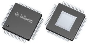
  • 64-Pin TQFP Package for the -4F/8F derivatives, 0.5 mm (19.7 mil) pitch (RoHS compliant)
Характеристики

Schedule_b

8542390000

Number_of_timers

5

Operating_temperature

-40 to 85 °C

Pin_count

64

Product_dimensions

10 x 10 x 1.4 mm

Program_memory_size

8 KB

Program_memory_type

Flash

Ram_size

0.75 KB

Screening_level

Industrial

On_chip_adc

14-chx8/10-bit

Specifications

https://4donline.ihs.com/images/VipMasterIC/IC/INFN/INFNS10464/INFNS10464-1.pdf?hkey=52A5661711E402568146F3353EA87419

Supplier_package

TQFP

Watchdog

2

Max_speed

40 MHz

Operating_supply_voltage

2.5, 5 V

Instruction_set_architecture

CISC, DSP, RISC

Бренд

Country_of_origin

United States

Data_bus_width

16 Bit

Device_core

C166S V2

Eccn

EAR99

Htsn

8542310001

Тип интерфейса

SPI/USART

Number_of_programmable_i_os

47

Max_expanded_memory_size

16 MB

Max_operating_supply_voltage

2.7, 5.5 V

Max_processing_temp

260 °C

Min_operating_supply_voltage

2.35, 4.4 V

Mounting

Surface Mount

Msl_level

3

Артикул: SAF-XC164TM-8F40FAA

Описание

The XC164TM derivatives are high-performance members of the Infineon XC166 Family of full featured single-chip CMOS microcontrollers. These devices extend the functionality and performance of the C166 Family in terms of instructions (MAC unit), peripherals, and speed. They combine high CPU performance (up to 40 million instructions per second) with high peripheral functionality and enhanced IO-capabilities. They also provide clock generation via PLL and various on-chip memory modules such as program Flash, program RAM, and data RAM.

  • High Performance 16-bit CPU with 5-Stage Pipeline
    • 25 ns Instruction Cycle Time at 40 MHz CPU Clock (Single-Cycle Execution)
    • 1-Cycle Multiplication (16 × 16 bit), Background Division (32 / 16 bit) in 21 Cycles
    • 1-Cycle Multiply-and-Accumulate (MAC) Instructions
    • Enhanced Boolean Bit Manipulation Facilities
    • Zero-Cycle Jump Execution
    • Additional Instructions to Support HLL and Operating Systems
    • Register-Based Design with Multiple Variable Register Banks
    • Fast Context Switching Support with Two Additional Local Register Banks
    • 16 Mbytes Total Linear Address Space for Code and Data
    • 1024 Bytes On-Chip Special Function Register Area (C166 Family Compatible)
  • 16-Priority-Level Interrupt System with up to 63 Sources, Sample-Rate down to 50 ns
  • 8-Channel Interrupt-Driven Single-Cycle Data Transfer Facilities via Peripheral Event Controller (PEC), 24-Bit Pointers Cover Total Address Space
  • Clock Generation via on-chip PLL (factors 1:0.15 … 1:10), or via Prescaler (factors 1:1 … 60:1)
  • On-Chip Memory Modules
    • 2 Kbytes On-Chip Dual-Port RAM (DPRAM)
    • 0/2/4 Kbytes1) On-Chip Data SRAM (DSRAM)
    • 2 Kbytes On-Chip Program/Data SRAM (PSRAM)
    • 32/64/1281) Kbytes On-Chip Program Memory (Flash Memory)
  • On-Chip Peripheral Modules
    • 14-Channel A/D Converter with Programmable Resolution (10-bit or 8-bit) and Conversion Time (down to 2.55 µs or 2.15 µs)
    • 16-Channel General Purpose Capture/Compare Unit (CAPCOM2)
    • Multi-Functional General Purpose Timer Unit with 5 Timers
    • Two Synchronous/Asynchronous Serial Channels (USARTs)
    • Two High-Speed-Synchronous Serial Channels
    • On-Chip Real Time Clock, Driven by the Main Oscillator
  • Idle, Sleep, and Power Down Modes with Flexible Power Management
  • Programmable Watchdog Timer and Oscillator Watchdog
  • Up to 47 General Purpose I/O Lines, partly with Selectable Input Thresholds and Hysteresis
  • On-Chip Bootstrap Loader
  • On-Chip Debug Support via JTAG Interface
  • 64-Pin Green LQFP Package for the -16F derivatives, 0.5 mm (19.7 mil) pitch (RoHS compliant)
  • 64-Pin TQFP Package for the -4F/8F derivatives, 0.5 mm (19.7 mil) pitch (RoHS compliant)
Детали

Schedule_b

8542390000

Number_of_timers

5

Operating_temperature

-40 to 85 °C

Pin_count

64

Product_dimensions

10 x 10 x 1.4 mm

Program_memory_size

8 KB

Program_memory_type

Flash

Ram_size

0.75 KB

Screening_level

Industrial

On_chip_adc

14-chx8/10-bit

Specifications

https://4donline.ihs.com/images/VipMasterIC/IC/INFN/INFNS10464/INFNS10464-1.pdf?hkey=52A5661711E402568146F3353EA87419

Supplier_package

TQFP

Watchdog

2

Max_speed

40 MHz

Operating_supply_voltage

2.5, 5 V

Instruction_set_architecture

CISC, DSP, RISC

Бренд

Country_of_origin

United States

Data_bus_width

16 Bit

Device_core

C166S V2

Eccn

EAR99

Htsn

8542310001

Тип интерфейса

SPI/USART

Number_of_programmable_i_os

47

Max_expanded_memory_size

16 MB

Max_operating_supply_voltage

2.7, 5.5 V

Max_processing_temp

260 °C

Min_operating_supply_voltage

2.35, 4.4 V

Mounting

Surface Mount

Msl_level

3