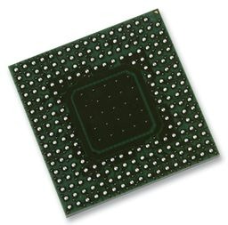
The ST10F280 is a new derivative of the STMicroelectronics ST10 family of 16-bit single-chip CMOS microcontrollers. It combines high CPU performance (up to 20 million instructions per second) with high peripheral functionality and enhanced I/O-capabilities. It also provides on-chip high-speed single voltage FLASH memory, on-chip high-speed RAM, and clock generation via PLL.ST10F280 is processed in 0.35µm CMOS technology. The MCU core and the logic is supplied with a 5V to 3.3V on chip voltage regulator. The part is supplied with a single 5V supply and I/Os work at 5V.The device is upward compatible with the ST10F269 device, with the following set of differences:Two supply pins (DC1,DC2) on the PBGA-208 package are used for decoupling the internally generated 3.3V core logic supply. Do not connect these two pins to 5.0V external supply. Instead, these pins should be connected to a decoupling capacitor (ceramic type, value = 330nF).The A/D Converter characteristics stay identical but 16 new input channel are added. A bit in a new register (XADCMUX) control the multiplexage between the first block of 16 channel (on Port5) and the second block (on XPort10). The conversion result registers stay identical and the software management can determine the block in use. A new dedicated timer controls now the ADC channel injection mode on the input CC31 (P7.7). The output of this timer is visible on a dedicated pin (XADCINJ) to emulate this new functionnality.A second XPWM peripheral (4 new channels) is added. Four dedicated pins are reserved for the outputs (XPWM[0:3])A new general purpose I/O port named XPORT9 (16 bits) is added. Due to the bit addressing management, it will be different from other standard general purpose I/O ports.
High performance cpu with dsp functions
16-bit CPU with 4-stage pipeline.
50ns Instruction cycle time at 40MHz CPU clock
Multiply/accumulate unit (MAC) 16 x 16-bit multiplication, 40-bit accumulator
Repeat unit
Enhanced boolean bit manipulation facilities
Additional instructions to support hll and operating systems
Single-cycle context switching support
Memory organization
512KB on-chip Flash memory single voltage with erase/program controller
100K erasing/programming cycles
20 year data retention time
Up to 16MB linear address space for code and data (5MB with CAN)
2KB on-chip internal ram (IRAM)
16KB extension RAM (XRAM)
Fast and flexible bus
Programmable external bus characteristics for different address ranges
8-bit or 16-bit external data bus
Multiplexed or demultiplexed external address/data buses
Five programmable chip-select signals
Hold-acknowledge bus arbitration support
Interrupt
8-channel peripheral event controller for single cycle, interrupt driven data transfer
16-priority-level interrupt system with 56 sources, sample-rate down to 25ns
Two multi-functional general purpose timer units with 5 timers
Two 16-channel capture/compare units
A/D converter
2X16-channel 10-bit
4.85µs conversion time
One timer for adc channel injection
8-channel PWM unit
Serial channels
Synchronous/async serial channel
High-speed synchronous channel
Fail-safe protection
Programmable watchdog timer
Oscillator watchdog
Two CAN 2.0b interfaces operating on one or two can busses (30 or 2×15 message objects)
On-chip bootstrap loader
Clock generation
On-chip PLL
Direct or prescaled clock input
Up to 143 general purpose i/o lines
Individually programmable as input, output or special function
Programmable threshold (hysteresis)
Idle and power down modes
Maximum cpu frequency 40MHz
Package PBGA 208 balls (23 x 23 x 1.96 mm – pitch 1.27 mm)
Single voltage supply: 5 V ±10% (embedded regulator for 3.3 V core supply)
Temperature range: -40°C to 125°C
