MCU 16-Bit S12 S12Z CISC 32KB Flash 9V/12V/15V 32-Pin LQFP Brick, S9S12ZVL32F0MLC, NXP

The MC9S12ZVL-Family is an automotive 16-bit microcontroller family using the 180nm NVM + UHV technology that offers the capability to integrate 40V analog components. This family reuses many features from the existing S12 portfolio. The particular differentiating features of this family are the enhanced S12Z core and the integration of “high-voltage” analog modules, including the voltage regulator (VREG) and a Local Interconnect Network (LIN) physical layer. The MC9S12ZVL-Family includes error correction code (ECC) on RAM, FLASH and EEPROM for diagnostic or data storage, a fast analog-to-digital converter (ADC) and a frequency modulated phase locked loop (IPLL) that improves the EMC performance. The MC9S12ZVL-Family delivers an optimized solution with the integration of several key system components into a single device, optimizing system architecture and achieving significant space savings. The MC9S12ZVL-Family delivers all the advantages and efficiencies of a 16-bit MCU while retaining the low cost, power consumption, EMC, and code-size efficiency advantages currently enjoyed by users of existing S12 families. The MC9S12ZVL-Family is available in 48-pin, 32-pin LQFP and 32-pin QFN-EP. In addition to the I/O ports available in each module, further I/O ports are available with interrupt capability allowing wake-up from stop or wait modes. The MC9S12ZVL-Family is a general-purpose family of devices suitable for a wide range of applications. The MC9S12ZVL-Family is targeted at generic automotive applications requiring LIN connectivity. Typical examples of these applications include switch panels and body endpoints for sensors.

  • S12Z CPU core
  • 32, 16 or 8 KB on-chip flash with ECC
  • 128 byte EEPROM with ECC
  • 1024 or 512 byte on-chip SRAM with ECC
  • Phase locked loop (IPLL) frequency multiplier with internal filter
  • 1 MHz internal RC oscillator with +/-1.3% accuracy over rated temperature range
  • 4-20 MHz amplitude controlled pierce oscillator
  • Internal COP (watchdog) module
  • analog-to-digital converter (ADC) with 10 -bit resolution and up to 10 channels available on external pins and Vbg (bandgap) result reference
  • One serial peripheral interface (SPI) module
  • One serial communication interface (SCI) module with interface to internal LIN physical layer transceiver (with RX connected to a timer channel for frequency calibration purposes, if desired)
  • Up to one additional SCI (not connected to LIN physical layer)
  • One on-chip LIN physical layer transceiver fully compliant with the LIN 2.2 standard
  • 6-channel timer module (TIM0) with input capture/output compare
  • 2-channel timer module (TIM1) with input capture/output compare
  • Inter-IC (IIC) module
  • 8-channel Pulse Width Modulation module (PWM)
  • On-chip voltage regulator (VREG) for regulation of input supply and all internal voltages
  • Autonomous periodic interrupt (API), supports cyclic wakeup from Stop mode
  • Pins to support 25 mA drive strength to VSSX
  • Pin to support 20 mA drive strength from VDDX (EVDD)
  • High Voltage Input (HVI)
  • Supply voltage sense with low battery warning
  • On-chip temperature sensor, temperature value can be measured with ADC or can generate an high temperature warning
  • Up to 23 pins can be used as keyboard wake-up interrupt (KWI)
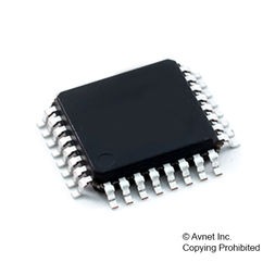
Характеристики

Schedule_b

8542310000

Бренд

Operating_temperature

-40 to 125 °C

Pin_count

32

Product_dimensions

7 x 7 x 1.4

Program_memory_size

32 Kb

Program_memory_type

Flash

Ram_size

1 KB

Screening_level

Automotive

On_chip_adc

10-chx10-bit

Specifications

https://4donline.ihs.com/images/VipMasterIC/IC/PHGL/PHGL-S-A0003296837/PHGL-S-A0003296837-1.pdf?hkey=52A5661711E402568146F3353EA87419

Supplier_package

LQFP

Watchdog

1

Max_speed

32 MHz

Number_of_timers

2

Operating_supply_voltage

9, 12, 15 V

Country_of_origin

China

Instruction_set_architecture

CISC

Data_bus_width

16 Bit

Data_memory_size

128 KB

Device_core

S12Z

Eccn

3A991.A.2

Htsn

8542310001

Тип интерфейса

I2C/SCI/SPI

Number_of_programmable_i_os

19

Lead_finish

Matte Tin

Max_expanded_memory_size

16 MB

Max_operating_supply_voltage

18 V

Max_processing_temp

260

Min_operating_supply_voltage

5.5 V

Mounting

Surface Mount

Msl_level

3

SKU: S9S12ZVL32F0MLC

Description

The MC9S12ZVL-Family is an automotive 16-bit microcontroller family using the 180nm NVM + UHV technology that offers the capability to integrate 40V analog components. This family reuses many features from the existing S12 portfolio. The particular differentiating features of this family are the enhanced S12Z core and the integration of “high-voltage” analog modules, including the voltage regulator (VREG) and a Local Interconnect Network (LIN) physical layer. The MC9S12ZVL-Family includes error correction code (ECC) on RAM, FLASH and EEPROM for diagnostic or data storage, a fast analog-to-digital converter (ADC) and a frequency modulated phase locked loop (IPLL) that improves the EMC performance. The MC9S12ZVL-Family delivers an optimized solution with the integration of several key system components into a single device, optimizing system architecture and achieving significant space savings. The MC9S12ZVL-Family delivers all the advantages and efficiencies of a 16-bit MCU while retaining the low cost, power consumption, EMC, and code-size efficiency advantages currently enjoyed by users of existing S12 families. The MC9S12ZVL-Family is available in 48-pin, 32-pin LQFP and 32-pin QFN-EP. In addition to the I/O ports available in each module, further I/O ports are available with interrupt capability allowing wake-up from stop or wait modes. The MC9S12ZVL-Family is a general-purpose family of devices suitable for a wide range of applications. The MC9S12ZVL-Family is targeted at generic automotive applications requiring LIN connectivity. Typical examples of these applications include switch panels and body endpoints for sensors.

  • S12Z CPU core
  • 32, 16 or 8 KB on-chip flash with ECC
  • 128 byte EEPROM with ECC
  • 1024 or 512 byte on-chip SRAM with ECC
  • Phase locked loop (IPLL) frequency multiplier with internal filter
  • 1 MHz internal RC oscillator with +/-1.3% accuracy over rated temperature range
  • 4-20 MHz amplitude controlled pierce oscillator
  • Internal COP (watchdog) module
  • analog-to-digital converter (ADC) with 10 -bit resolution and up to 10 channels available on external pins and Vbg (bandgap) result reference
  • One serial peripheral interface (SPI) module
  • One serial communication interface (SCI) module with interface to internal LIN physical layer transceiver (with RX connected to a timer channel for frequency calibration purposes, if desired)
  • Up to one additional SCI (not connected to LIN physical layer)
  • One on-chip LIN physical layer transceiver fully compliant with the LIN 2.2 standard
  • 6-channel timer module (TIM0) with input capture/output compare
  • 2-channel timer module (TIM1) with input capture/output compare
  • Inter-IC (IIC) module
  • 8-channel Pulse Width Modulation module (PWM)
  • On-chip voltage regulator (VREG) for regulation of input supply and all internal voltages
  • Autonomous periodic interrupt (API), supports cyclic wakeup from Stop mode
  • Pins to support 25 mA drive strength to VSSX
  • Pin to support 20 mA drive strength from VDDX (EVDD)
  • High Voltage Input (HVI)
  • Supply voltage sense with low battery warning
  • On-chip temperature sensor, temperature value can be measured with ADC or can generate an high temperature warning
  • Up to 23 pins can be used as keyboard wake-up interrupt (KWI)

Additional information

Schedule_b

8542310000

Бренд

Operating_temperature

-40 to 125 °C

Pin_count

32

Product_dimensions

7 x 7 x 1.4

Program_memory_size

32 Kb

Program_memory_type

Flash

Ram_size

1 KB

Screening_level

Automotive

On_chip_adc

10-chx10-bit

Specifications

https://4donline.ihs.com/images/VipMasterIC/IC/PHGL/PHGL-S-A0003296837/PHGL-S-A0003296837-1.pdf?hkey=52A5661711E402568146F3353EA87419

Supplier_package

LQFP

Watchdog

1

Max_speed

32 MHz

Number_of_timers

2

Operating_supply_voltage

9, 12, 15 V

Country_of_origin

China

Instruction_set_architecture

CISC

Data_bus_width

16 Bit

Data_memory_size

128 KB

Device_core

S12Z

Eccn

3A991.A.2

Htsn

8542310001

Тип интерфейса

I2C/SCI/SPI

Number_of_programmable_i_os

19

Lead_finish

Matte Tin

Max_expanded_memory_size

16 MB

Max_operating_supply_voltage

18 V

Max_processing_temp

260

Min_operating_supply_voltage

5.5 V

Mounting

Surface Mount

Msl_level

3