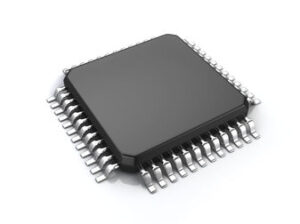
MCU 16-bit R8C CISC 48KB Flash 3.3V/5V 48-Pin LQFP, M30260F6AGP#U3A, Renesas Electronics

The M16C/26A is based on the M16C/60 CPU Core. Maximum operating frequencyis 24MHz when using PLL Synthesizer. Flash Memory Version. Internal Flash Memory is programmable on a single power source.

  • 16-bit Multifunction Timer (Timer A and B, incl. 3-phase inverter motorcontrol function): 8 channels
  • UART/Clock Synchronous Serial Interface: 3 channels
  • 10-bit A/D Converter: 12 channels
  • DMAC: 2 channels
  • CRC Calculation Circuit
  • Watchdog Timer
  • Clock Generation Circuits: Main Clock Generation Circuit, Sub ClockGeneration Circuit, On-chip Oscillator, PLL Synthesizer
  • Oscillation Stop Detection Function
  • Voltage Detection Circuit
  • I/O Ports: 39
  • External Interrupt Pins: 11
  • Data Flash: 2KB × 2 blocks

Характеристики

Schedule_b

8542310000

Number_of_timers

8

Operating_temperature

-40 to 85 °C

Pin_count

48

Product_dimensions

7 x 7 x 1.4 mm

Screening_level

Industrial

On_chip_adc

12-chx10-bit

Specifications

https://4donline.ihs.com/images/VipMasterIC/IC/RNCC/RNCCS00915/RNCCS00043-1.pdf?hkey=52A5661711E402568146F3353EA87419

Supplier_package

LQFP

Watchdog

1

Max_speed

20 MHz

Operating_supply_voltage

3.3, 5 V

Instruction_set_architecture

CISC

Бренд

Data_bus_width

16 Bit

Eccn

EAR99

Htsn

8542310001

Тип интерфейса

UART

Number_of_programmable_i_os

39

Lead_finish

Tin/Copper

Max_expanded_memory_size

1 MB

Max_processing_temp

260 °C

Mounting

Surface Mount

Msl_level

3

SKU: M30260F6AGP#U3A

Description

The M16C/26A is based on the M16C/60 CPU Core. Maximum operating frequencyis 24MHz when using PLL Synthesizer. Flash Memory Version. Internal Flash Memory is programmable on a single power source.

  • 16-bit Multifunction Timer (Timer A and B, incl. 3-phase inverter motorcontrol function): 8 channels
  • UART/Clock Synchronous Serial Interface: 3 channels
  • 10-bit A/D Converter: 12 channels
  • DMAC: 2 channels
  • CRC Calculation Circuit
  • Watchdog Timer
  • Clock Generation Circuits: Main Clock Generation Circuit, Sub ClockGeneration Circuit, On-chip Oscillator, PLL Synthesizer
  • Oscillation Stop Detection Function
  • Voltage Detection Circuit
  • I/O Ports: 39
  • External Interrupt Pins: 11
  • Data Flash: 2KB × 2 blocks

Additional information

Schedule_b

8542310000

Number_of_timers

8

Operating_temperature

-40 to 85 °C

Pin_count

48

Product_dimensions

7 x 7 x 1.4 mm

Screening_level

Industrial

On_chip_adc

12-chx10-bit

Specifications

https://4donline.ihs.com/images/VipMasterIC/IC/RNCC/RNCCS00915/RNCCS00043-1.pdf?hkey=52A5661711E402568146F3353EA87419

Supplier_package

LQFP

Watchdog

1

Max_speed

20 MHz

Operating_supply_voltage

3.3, 5 V

Instruction_set_architecture

CISC

Бренд

Data_bus_width

16 Bit

Eccn

EAR99

Htsn

8542310001

Тип интерфейса

UART

Number_of_programmable_i_os

39

Lead_finish

Tin/Copper

Max_expanded_memory_size

1 MB

Max_processing_temp

260 °C

Mounting

Surface Mount

Msl_level

3