Описание
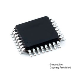
The R8C/27 is based on the R8C CPU Core. Maximum operating frequency is 20 MHz. A Flash Memory Version is available. Internal Flash Memory is programmable on a single power source.
- 8-bit Multifunction Timer with 8-bit prescaler (Timer RA and RB): 2 channels
- Input Capture/Output Compare Timer (Timer RC): 16-bit x 1 channel
- Real-Time Clock Timer with compare match function (Timer RE): 1 channel
- UART/Clock Synchronous Serial Interface: 2 channels
- I2C-bus Interface (IIC)/Chip-select Clock Synchronous Serial Interface: 1 channel
- LIN Module: 1 channel (Timer RA, UART0)
- 10-bit A/D Converter: 12 channels
- Watchdog Timer
- Clock Generation Circuits: XIN Clock Generation Circuit, On-chip Oscillator (High/Low Speed), XCIN Clock Generation Circuit
- Oscillation Stop Detection Function
- Voltage Detection Circuit
- Power-On Reset Circuit
- I/O Ports: 25 (incl. LED drive ports)
- External Interrupt Pins: 7
- Data Flash: 2 KB